-
ADS1220 4-Channel, 2-kSPS, Low-Power, 24-Bit ADC with Integrated PGA and Reference
- 1 Features
- 2 Applications
- 3 Description
- 4 Revision History
- 5 Pin Configuration and Functions
- 6 Specifications
- 7 Parameter Measurement Information
-
8 Detailed Description
- 8.1 Overview
- 8.2 Functional Block Diagram
- 8.3 Feature Description
- 8.4 Device Functional Modes
- 8.5 Programming
- 8.6 Register Map
- 9 Application and Implementation
- 10Power Supply Recommendations
- 11Layout
- 12Device and Documentation Support
- 13Mechanical, Packaging, and Orderable Information
- IMPORTANT NOTICE
Package Options
Mechanical Data (Package|Pins)
Thermal pad, mechanical data (Package|Pins)
- RVA|16
Orderable Information
ADS1220 4-Channel, 2-kSPS, Low-Power, 24-Bit ADC with Integrated PGA and Reference
1 Features
- Low Current Consumption:
As Low as 120 μA (typ) in Duty-Cycle Mode - Wide Supply Range: 2.3 V to 5.5 V
- Programmable Gain: 1 V/V to 128 V/V
- Programmable Data Rates: Up to 2 kSPS
- Up to 20-Bits Effective Resolution
- Simultaneous 50-Hz and 60-Hz Rejection at
20 SPS with Single-Cycle Settling Digital Filter - Two Differential or Four Single-Ended Inputs
- Dual Matched Programmable Current Sources:
10 μA to 1.5 mA - Internal 2.048-V Reference: 5 ppm/°C (typ) Drift
- Internal 2% Accurate Oscillator
- Internal Temperature Sensor:
0.5°C (typ) Accuracy - SPI-Compatible Interface (Mode 1)
- Package: 3.5-mm × 3.5-mm × 0.9-mm VQFN
2 Applications
- Temperature Sensor Measurements:
- Thermistors
- Thermocouples
- Resistance Temperature Detectors (RTDs):
2-, 3-, or 4-Wire Types
- Resistive Bridge Sensor Measurements:
- Pressure Sensors
- Strain Gauges
- Weigh Scales
- Portable Instrumentation
- Factory Automation and Process Control
3 Description
The ADS1220 is a precision, 24-bit, analog-to-digital converter (ADC) that offers many integrated features to reduce system cost and component count in applications measuring small sensor signals. The device features two differential or four single-ended inputs through a flexible input multiplexer (MUX), a low-noise, programmable gain amplifier (PGA), two programmable excitation current sources, a voltage reference, an oscillator, a low-side switch, and a precision temperature sensor.
The device can perform conversions at data rates up to 2000 samples-per-second (SPS) with single-cycle settling. At 20 SPS, the digital filter offers simultaneous 50-Hz and 60-Hz rejection for noisy industrial applications. The internal PGA offers gains up to 128 V/V. This PGA makes the ADS1220 ideally-suited for applications measuring small sensor signals, such as resistance temperature detectors (RTDs), thermocouples, thermistors, and resistive bridge sensors. The device supports measurements of pseudo- or fully-differential signals when using the PGA. Alternatively, the device can be configured to bypass the internal PGA while still providing high input impedance and gains up to 4 V/V, allowing for single-ended measurements.
Power consumption is as low as 120 µA when operating in duty-cycle mode with the PGA disabled. The ADS1220 is offered in a leadless VQFN-16 or a TSSOP-16 package and is specified over a temperature range of –40°C to +125°C.
Device Information(1)
| PART NUMBER | PACKAGE | BODY SIZE (NOM) |
|---|---|---|
| ADS1220 | VQFN (16) | 3.50 mm × 3.50 mm |
| TSSOP (16) | 5.00 mm × 4.40 mm |
- For all available packages, see the orderable addendum at the end of the data sheet.
4 Revision History
Changes from B Revision (February 2015) to C Revision
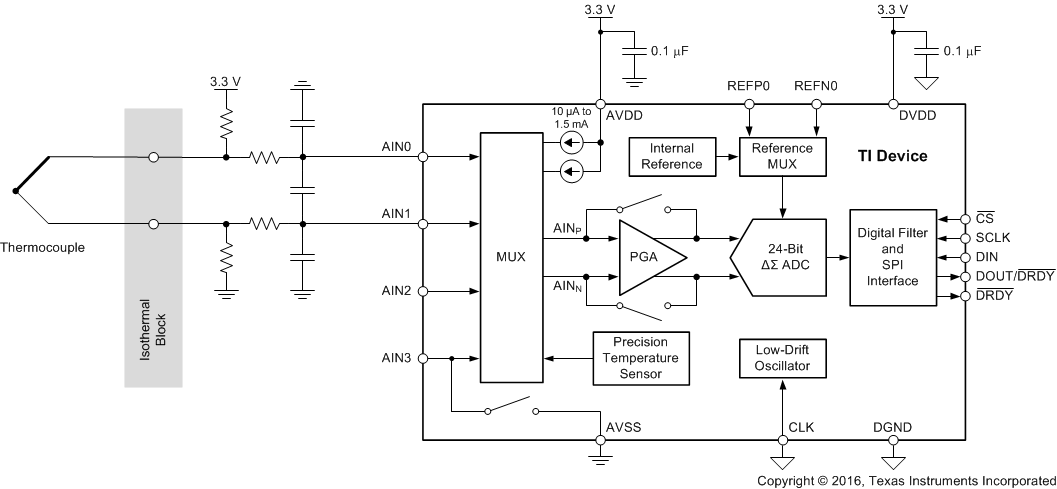
- Changed K-Type Thermocouple Measurement figureGo
- Added footnote 1 to Pin Functions table and changed descriptions of AIN0/REFP1, AIN1, AIN2, AIN3/REFN1, REFN0, and REFP0 pins accordinglyGo
- Changed Functional Block Diagram figureGo
- Changed Bypassing the PGA sectionGo
- Added fourth sentence to Temperature Sensor sectionGo
- Changed last equation in Converting from Digital Codes to Temperature sectionGo
- Changed description of bits 5:4 in Configuration Register 2Go
- Added Unused Inputs and Outputs section Go
- Changed Figure 74Go
- Changed Figure 77Go
- Changed Figure 78Go
- Changed Figure 79Go
- Changed Figure 82Go
- Changed Power Supply Recommendations section: changed Power-Supply Sequencing subsection, added Power-Supply Ramp Rate subsectionGo
Changes from A Revision (July 2013) to B Revision
- Added TI Design, Device Information, ESD Ratings, Recommended Operating Conditions, and Switching Characteristics tables and Application and Implementation, Power Supply Recommendations, Layout, Device and Documentation Support, and Mechanical, Packaging, and Orderable Information sectionsGo
- Changed document title, QFN to VQFN throughout document, Features, Applications, Description, Pin Configuration and Functions, Parameter Measurement Information, Feature Description, Device Functional Modes, Programming, and Register Map sections, and front-page figureGo
- Deleted Product Family table Go
- Changed format of Absolute Maximum Ratings table, added minimum junction temperature specification, changed input current parameter name, and removed momentary input current specificationGo
- Changed Analog Inputs and Voltage Reference Inputs sections (specification values were not changed) and added Internal Oscillator section to Electrical Characteristics tableGo
- Changed System Performance section: changed VIO parameter name and added PGA disabled row to Offset drift, Gain error, and Gain drift parameters in System Performance section of Electrical Characteristics tableGo
- Changed Internal Voltage Reference section: changed Reference drift parameter maximum specification and added Long-term drift parameter in Electrical Characteristics tableGo
- Deleted Clock Sources section and changed Temperature Sensor and Power Supply sections (specification values were not changed) in Electrical Characteristics tableGo
- Changed Digital Inputs/Outputs section, VIL parameter minimum specification in Electrical Characteristics tableGo
- Changed SPI Timing Requirements and Figure 1 (specification values were not changed), added SPI Switching Characteristics and Figure 2 Go
- Changed format of Typical Characteristics section (actual curves did not change)Go
Changes from * Revision (May 2013) to A Revision
- Changed document status to Mixed Status; pre-RTM changes made throughoutGo
