ADSxx53 Dual, High-Speed, 16-, 14-, and 12-Bit, Simultaneous-Sampling, Analog-to-Digital Converters
1 Features
- 16-, 14-, and 12-Bit, Pin-Compatible Family
- Simultaneous Sampling of Two Channels
- Supports Single-Ended and Pseudo-Differential Inputs
- High Speed:
- ADS8353: 16 Bits, 600 kSPS
- ADS7853: 14 Bits, 1 MSPS
- ADS7253: 12 Bits, 1 MSPS
- Excellent DC Performance:
- ADS8353:
- 16-Bit NMC DNL, ±2.5-LSB Max INL
- ADS7853:
- 14-Bit NMC DNL, ±2-LSB Max INL
- ADS7253:
- 12-Bit NMC DNL, ±1-LSB Max INL
- ADS8353:
- Excellent AC Performance:
- ADS8353:
- 89-dB SNR, –100-dB THD
- ADS7853:
- 82-dB SNR, –90-dB THD
- ADS7253:
- 72-dB SNR, –90-dB THD
- ADS8353:
- Dual, Programmable, and Buffered
2.5-V Internal Reference - Fully-Specified Over the Extended Industrial Temperature Range: –40°C to 125°C
- Small Footprint:
WQFN-16 (3-mm × 3-mm) and TSSOP-16
2 Applications
- Motor Control:
Position Measurement Using Encoders - Optical Networking: EDFA Gain Control Loops
- Protection Relays
- Power Quality Measurement
- Three-Phase Power Controls
- Programmable Logic Controllers
3 Description
The ADS8353, ADS7853, and ADS7253 belong to a family of pin-compatible, dual, high-speed, simultaneous-sampling, analog-to-digital converters (ADCs) that support single-ended and pseudo-differential analog inputs.
Each device includes two individually programmable reference sources that can be used for system-level gain calibration. Also, a flexible serial interface that can operate over a wide power-supply range enables easy communication with a large variety of host controllers. Power consumption for a given throughput can be optimized by using the two low-power modes supported by the device. All devices are fully specified over the extended industrial temperature range (–40°C to 125°C) and are available in pin-compatible, WQFN-16 (3-mm ×
3-mm) and TSSOP-16 packages.
Device Information(1)
| PART NUMBER | PACKAGE | BODY SIZE (NOM) |
|---|---|---|
| ADSxx53 | TSSOP (16) | 5.00 mm × 4.40 mm |
| WQFN (16) | 3.00 mm × 3.00 mm |
- For all available packages, see the orderable addendum at the end of the datasheet.
Typical Application Diagram
4 Revision History
Changes from A Revision (July 2014) to B Revision
- Made changes to the ADS8353 preview device and moved to Production Data statusGo
- Changed document status from Mixed Status to Production DataGo
- Corrected cross-reference for Figure 99Go
Changes from * Revision (October 2013) to A Revision
- Made changes to product preview data sheetGo
5 Device Comparison Table
| PRODUCT | RESOLUTION (Bits) | INPUT CONFIGURATION | NMC (Bits) | INL (LSB) | SNR (dB) |
|---|---|---|---|---|---|
| ADS8354 | 16 | Fully-differential | 16 | ±2.5 | 93 (typ) |
| ADS7854 | 14 | Fully-differential | 14 | ±1.5 | 88 (typ) |
| ADS7254 | 12 | Fully-differential | 12 | ±1 | 74 (typ) |
| ADS8353 | 16 | Single-ended and pseudo-differential |
16 | ±2.5 | 89 (typ) |
| ADS7853 | 14 | Single-ended and pseudo-differential |
14 | ±2 | 84 (typ) |
| ADS7253 | 12 | Single-ended and pseudo-differential |
12 | ±1 | 73.5 (typ) |
6 Pin Configurations and Functions

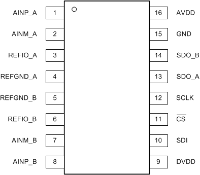
Pin Functions
| PIN | I/O | DESCRIPTION | ||
|---|---|---|---|---|
| NAME | NO. | |||
| TSSOP | WQFN | |||
| AINM_A | 2 | 16 | Analog input | Negative analog input, channel A |
| AINM_B | 7 | 5 | Analog input | Negative analog input, channel B |
| AINP_A | 1 | 15 | Analog input | Positive analog input, channel A |
| AINP_B | 8 | 6 | Analog input | Positive analog input, channel B |
| AVDD | 16 | 14 | Supply | Supply voltage for ADC operation |
| CS | 11 | 9 | Digital input | Chip-select signal; active low |
| DVDD | 9 | 7 | Digital I/O supply | Digital I/O supply |
| GND | 15 | 13 | Supply | Digital ground |
| REFGND_A | 4 | 2 | Supply | Reference ground potential A |
| REFGND_B | 5 | 3 | Supply | Reference ground potential B |
| REFIO_A | 3 | 1 | Analog input/output | Reference voltage input/output, channel A |
| REFIO_B | 6 | 4 | Analog input/output | Reference voltage input/output, channel B |
| SCLK | 12 | 10 | Digital input | Clock for serial communication |
| SDI | 10 | 8 | Digital input | Data input for serial communication |
| SDO_A | 13 | 11 | Digital output | Data output for serial communication, channel A and channel B |
| SDO_B | 14 | 12 | Digital output | Data output for serial communication, channel B |
| Thermal pad | — | Thermal pad | Supply | Exposed thermal pad (only for WQFN). TI recommends connecting this pin to the printed circuit board (PCB) ground. |
7 Specifications
7.1 Absolute Maximum Ratings(1)
over operating free-air temperature range (unless otherwise noted)| MIN | MAX | UNIT | ||
|---|---|---|---|---|
| AVDD to REFGND_x or DVDD to GND | –0.3 | 6 | V | |
| Analog (AINP_x and AINM_x) and reference input (REFIO_x) voltage with respect to REFGND_x | REFGND_x – 0.3 | AVDD + 0.3 | V | |
| Digital input voltage with respect to GND | GND – 0.3 | DVDD + 0.3 | V | |
| Ground voltage difference |REFGND_x-GND| | 0.3 | V | ||
| Input current to any pin except supply pins | ±10 | mA | ||
| Maximum virtual junction temperature, TJ | 150 | °C | ||
7.2 Handling Ratings
| MIN | MAX | UNIT | |||
|---|---|---|---|---|---|
| Tstg | Storage temperature range | –65 | 150 | °C | |
| V(ESD) | Electrostatic discharge | Human body model (HBM), per ANSI/ESDA/JEDEC JS-001, all pins(1) | –2000 | 2000 | V |
| Charged device model (CDM), per JEDEC specification JESD22-C101, all pins(2) | –500 | 500 | |||
7.3 Recommended Operating Conditions
over operating free-air temperature range (unless otherwise noted)| MIN | NOM | MAX | UNIT | ||
|---|---|---|---|---|---|
| AVDD | Analog supply voltage | 5 | V | ||
| DVDD | Digital supply voltage | 3.3 | V | ||
7.4 Thermal Information
| THERMAL METRIC(1) | ADS8353, ADS7853, ADS7253 | UNIT | ||
|---|---|---|---|---|
| RTE (WQFN) | PW (TSSOP) | |||
| 16 PINS | 16 PINS | |||
| RθJA | Junction-to-ambient thermal resistance | 33.3 | 86.9 | °C/W |
| RθJC(top) | Junction-to-case (top) thermal resistance | 29.5 | 21 | |
| RθJB | Junction-to-board thermal resistance | 7.3 | 39.1 | |
| ψJT | Junction-to-top characterization parameter | 0.2 | 0.8 | |
| ψJB | Junction-to-board characterization parameter | 7.4 | 38.4 | |
| RθJC(bot) | Junction-to-case (bottom) thermal resistance | 0.9 | N/A | |
7.5 Electrical Characteristics: ADS8353
All minimum and maximum specifications are at TA = –40°C to 125°C, AVDD = 5 V, DVDD = 3.3 V, VREF_A = VREF_B = VREF = 2.5 V (internal), and fDATA = 600 kSPS, unless otherwise noted.Typical values are at TA = 25°C, AVDD = 5 V, and DVDD = 3.3 V.
| PARAMETER | TEST CONDITIONS | MIN | TYP | MAX | UNIT | |
|---|---|---|---|---|---|---|
| RESOLUTION | ||||||
| Resolution | 16 | Bits | ||||
| DC ACCURACY(2) | ||||||
| NMC | No missing codes | 32-clock mode | 16 | Bits | ||
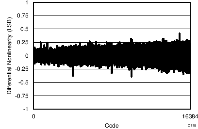
| INL | Integral nonlinearity | 32-clock mode | –2.5 | ±1 | 2.5 | LSB |
| DNL | Differential nonlinearity | 32-clock mode | –0.99 | ±0.6 | 2 | LSB |
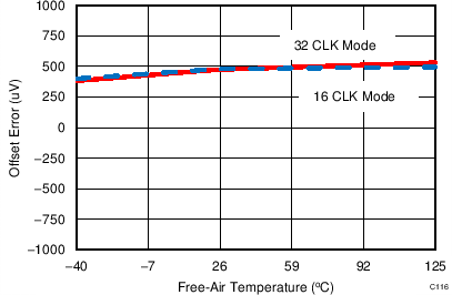
| EIO | Input offset error | –1 | ±0.5 | 1 | mV | |
| EIO match | ADC_A to ADC_B | –1 | ±0.5 | 1 | mV | |
| dEIO/dT | Input offset thermal drift | 1 | μV/°C | |||
| EG | Gain error | Referenced to the voltage at REFIO_x | –0.1 | ±0.05 | 0.1 | %FS |
| EG match | ADC_A to ADC_B | –0.1 | ±0.05 | 0.1 | %FS | |
| dEG/dT | Gain error thermal drift | Referenced to the voltage at REFIO_x | 1 | ppm/°C | ||
| AC ACCURACY(1) | ||||||
| SINAD | Signal-to-noise + distortion | VREF = 2.5 V, VREF input range, 32-clock mode |
80.2 | 83 | dB | |
| VREF = 2.5 V, 2 × VREF input range, 32-clock mode |
83.9 | dB | ||||
| VREF = 5 V (external), VREF input range, 32-clock mode |
88.7 | dB | ||||
| SNR | Signal-to-noise ratio | VREF = 2.5 V, VREF input range, 32-clock mode |
80.5 | 83 | dB | |
| VREF = 2.5 V, 2 × VREF input range, 32-clock mode |
84 | dB | ||||
| VREF = 5 V (external), VREF input range, 32-clock mode |
89 | dB | ||||
| THD | Total harmonic distortion | VREF = 2.5 V, VREF input range, 32-clock mode |
–100 | dB | ||
| VREF = 2.5 V, 2 × VREF input range, 32-clock mode |
–100 | dB | ||||
| VREF = 5 V (external), VREF input range, 32-clock mode |
–100 | dB | ||||
| SFDR | Spurious-free dynamic range | VREF = 2.5 V, VREF input range, 32-clock mode |
105 | dB | ||
| VREF = 2.5 V, 2 × VREF input range, 32-clock mode |
105 | dB | ||||
| VREF = 5 V (external), VREF input range, 32-clock mode |
105 | dB | ||||
7.6 Electrical Characteristics: ADS7853
All minimum and maximum specifications are at TA = –40°C to 125°C, AVDD = 5 V, DVDD = 3.3 V, VREF_A = VREF_B = VREF = 2.5 V (internal), and fDATA = 1 MSPS, unless otherwise noted.Typical values are at TA = 25°C, AVDD = 5 V, and DVDD = 3.3 V.
| PARAMETER | TEST CONDITIONS | MIN | TYP | MAX | UNIT | ||
|---|---|---|---|---|---|---|---|
| RESOLUTION | |||||||
| Resolution | 14 | Bits | |||||
| DC ACCURACY(2) | |||||||
| NMC | No missing codes | 32-clock mode | 14 | Bits | |||
| 16-clock mode | 13 | Bits | |||||
| INL | Integral nonlinearity | 32-clock mode | –2 | ±0.7 | 2 | LSB | |
| 16-clock mode | –2.5 | ±1 | 2.5 | LSB | |||
| DNL | Differential nonlinearity | 32-clock mode | –0.99 | ±0.5 | 1 | LSB | |
| 16-clock mode | –1 | ±0.9 | 2 | LSB | |||
| EIO | Input offset error | –1 | ±0.5 | 1 | mV | ||
| EIO match | ADC_A to ADC_B | –1 | ±0.5 | 1 | mV | ||
| dEIO/dT | Input offset thermal drift | ±1 | μV/°C | ||||
| EG | Gain error | Referenced to the voltage at REFIO_x | –0.1 | ±0.05 | 0.1 | %FS | |
| EG match | ADC_A to ADC_B | –0.1 | ±0.05 | 0.1 | %FS | ||
| dEG/dT | Gain error thermal drift | Referenced to the voltage at REFIO_x | ±1 | ppm/°C | |||
| AC ACCURACY(1) | |||||||
| SINAD | Signal-to-noise + distortion | VREF = 2.5 V, VREF input range |
32-clock mode | 78.4 | 80.9 | dB | |
| 16-clock mode | 80.3 | dB | |||||
| VREF = 2.5 V, 2 × VREF input range |
32-clock mode | 81.4 | dB | ||||
| 16-clock mode | 80.8 | dB | |||||
| VREF = 5 V (external), VREF input range |
32-clock mode | 83.9 | dB | ||||
| 16-clock mode | 82.9 | dB | |||||
| SNR | Signal-to-noise ratio | VREF = 2.5 V, VREF input range |
32-clock mode | 78.5 | 81 | dB | |
| 16-clock mode | 80.5 | dB | |||||
| VREF = 2.5 V, 2 × VREF input range |
32-clock mode | 81.5 | dB | ||||
| 16-clock mode | 81 | dB | |||||
| VREF = 5 V (external), VREF input range |
32-clock mode | 84 | dB | ||||
| 16-clock mode | 83.5 | dB | |||||
| THD | Total harmonic distortion | VREF = 2.5 V, VREF input range |
32-clock mode | –100 | dB | ||
| 16-clock mode | –93 | dB | |||||
| VREF = 2.5 V, 2 × VREF input range |
32-clock mode | –98 | dB | ||||
| 16-clock mode | –94 | dB | |||||
| VREF = 5 V (external), VREF input range |
32-clock mode | –102 | dB | ||||
| 16-clock mode | –92 | dB | |||||
| SFDR | Spurious-free dynamic range | VREF = 2.5 V, VREF input range |
32-clock mode | 100 | dB | ||
| 16-clock mode | 95 | dB | |||||
| VREF = 2.5 V, 2 × VREF input range |
32-clock mode | 100 | dB | ||||
| 16-clock mode | 95 | dB | |||||
| VREF = 5 V (external), VREF input range |
32-clock mode | 102 | dB | ||||
| 16-clock mode | 95 | dB | |||||
| ISOXT | ADC-to-ADC isolation | fIN = 15 kHz at 10 %FS, fNOISE = 25 kHz at FS |
–100 | dB | |||
7.7 Electrical Characteristics: ADS7253
All minimum and maximum specifications are at TA = –40°C to 125°C, AVDD = 5 V, DVDD = 3.3 V, VREF_A = VREF_B = VREF = 2.5 V (internal), and fDATA = 1 MSPS, unless otherwise noted.Typical values are at TA = 25°C, AVDD = 5 V, and DVDD = 3.3 V.
| PARAMETER | TEST CONDITIONS | MIN | TYP | MAX | UNIT | ||
|---|---|---|---|---|---|---|---|
| RESOLUTION | |||||||
| Resolution | 12 | Bits | |||||
| DC ACCURACY(2) | |||||||
| NMC | No missing codes | 12 | Bits | ||||
| INL | Integral nonlinearity | –1 | ±0.3 | 1 | LSB | ||
| DNL | Differential nonlinearity | –0.99 | ±0.3 | 1 | LSB | ||
| EIO | Input offset error | –2 | ±0.5 | 2 | mV | ||
| EIO match | ADC_A to ADC_B | –2 | ±0.5 | 2 | mV | ||
| dEIO/dT | Input offset thermal drift | ±1 | μV/°C | ||||
| EG | Gain error | Referenced to the voltage at REFIO_x | –0.2 | ±0.05 | 0.2 | %FS | |
| EG match | ADC_A to ADC_B | –0.2 | ±0.05 | 0.2 | %FS | ||
| dEG/dT | Gain error thermal drift | Referenced to the voltage at REFIO_x | ±1 | ppm/°C | |||
| AC ACCURACY(1) | |||||||
| SINAD | Signal-to-noise + distortion | VREF = 2.5 V, VREF input range |
71 | 72.9 | dB | ||
| VREF = 2.5 V, 2 × VREF input range |
72.9 | dB | |||||
| VREF = 5 V (external), VREF input range |
73.4 | dB | |||||
| SNR | Signal-to-noise ratio | VREF = 2.5 V, VREF input range |
71.5 | 73 | dB | ||
| VREF = 2.5 V, 2 × VREF input range |
73 | dB | |||||
| VREF = 5 V (external), VREF input range |
73.5 | dB | |||||
| THD | Total harmonic distortion | VREF = 2.5 V, VREF input range |
–90 | dB | |||
| VREF = 2.5 V, 2 × VREF input range |
–90 | dB | |||||
| VREF = 5 V (external), VREF input range |
–90 | dB | |||||
| SFDR | Spurious-free dynamic range | VREF = 2.5 V, VREF input range |
93.5 | dB | |||
| VREF = 2.5 V, 2 × VREF input range |
93.5 | dB | |||||
| VREF = 5 V (external), VREF input range |
93.5 | dB | |||||
| ISOXT | ADC-to-ADC isolation | fIN = 15 kHz at 10 %FS, fNOISE = 25 kHz at FS |
–80 | dB | |||
7.8 Electrical Characteristics: All Devices
All minimum and maximum specifications are at TA = –40°C to 125°C, AVDD = 5 V, DVDD = 3.3 V, VREF_A = VREF_B = VREF = 2.5 V, and fDATA = maximum, unless otherwise noted.Typical values are at TA = 25°C, AVDD = 5 V, and DVDD = 3.3 V.
| PARAMETER | TEST CONDITIONS | MIN | TYP | MAX | UNIT | ||
|---|---|---|---|---|---|---|---|
| ANALOG INPUT | |||||||
| FSR | Full-scale input range(1)
(AINP_x – AINM_x) |
VREF range | Single-ended input, AINM_x = GND |
0 | VREF | V | |
| Pseudo-differential input, AINM_x = +VREF / 2 |
–VREF / 2 | VREF / 2 | V | ||||
| 2 × VREF range | Single-ended input, AINM_x = GND, AVDD ≥ 2 × VREF |
0 | 2 × VREF | V | |||
| Pseudo-differential input, AINM_x = +VREF, AVDD ≥ 2 × VREF |
–VREF | VREF | V | ||||
| VINP | Absolute input voltage (AINP_x to REFGND) |
VREF range | 0 | VREF | V | ||
| 2 × VREF range, AVDD ≥ 2 × VREF | 0 | 2 × VREF | V | ||||
| VINM | Absolute input voltage (AINM_x to REFGND) |
VREF range | Single-ended input | –0.1 | 0.1 | V | |
| Pseudo-differential input | VREF / 2 – 0.1 | VREF / 2 | VREF / 2 + 0.1 | V | |||
| 2 × VREF range | Single-ended input, AVDD ≥ 2 × VREF | –0.1 | 0.1 | V | |||
| Pseudo-differential input, AVDD ≥ 2 × VREF | VREF – 0.1 | VREF | VREF + 0.1 | V | |||
| Ci | Input capacitance | In sample mode | 40 | pF | |||
| In hold mode | 4 | pF | |||||
| Ilkg(i) | Input leakage current | 0.1 | µA | ||||
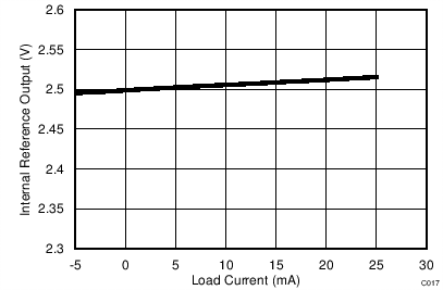
| INTERNAL VOLTAGE REFERENCE | |||||||
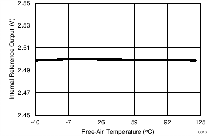
| VREFOUT | Reference output voltage | REFDAC_x = 1FFh (default), at 25°C |
2.495 | 2.500 | 2.505 | V | |
| VREF-match | VREF_A to VREF_B matching | REFDAC_x = 1FFh (default), at 25°C |
±1 | mV | |||
| REFDAC_x resolution(4) | 1.1 | mV | |||||
| dVREFOUT/dT | Reference voltage temperature drift | REFDAC_x = 1FFh (default) | ±10 | ppm/°C | |||
| dVREFOUT/dt | Long-term stability | 1000 hours | 150 | ppm | |||
| RO | Internal reference output impedance | 1 | Ω | ||||
| IREFOUT | Reference output dc current | 2 | mA | ||||
| CREFOUT | Recommended output capacitor | 10 | µF | ||||
| tREFON | Reference output settling time | For CREF = 10 μF | 8 | ms | |||
| VOLTAGE REFERENCE INPUT | |||||||
| VREF | Reference voltage (input) | VREF range | 2.4 | 2.5 | AVDD | V | |
| 2 × VREF range | 2.4 | 2.5 | AVDD / 2 | V | |||
| IREF | Average Reference input current | Per ADC | 300 | μA | |||
| CREF | External ceramic reference capacitance | 10 | μF | ||||
| Ilkg(dc) | DC leakage current | ±0.1 | μA | ||||
| SAMPLING DYNAMICS | |||||||
| tA | Aperture delay | 8 | ns | ||||
| tA match | ADC_A to ADC_B | 40 | ps | ||||
| tAJIT | Aperture jitter | 50 | ps | ||||
| DIGITAL INPUTS(2) | |||||||
| VIH | High-level input voltage | DVDD > 2.3 V | 0.7 DVDD | DVDD + 0.3 | V | ||
| DVDD ≤ 2.3 V | 0.8 DVDD | DVDD + 0.3 | V | ||||
| VIL | Low-level input voltage | DVDD > 2.3 V | –0.3 | 0.3 DVDD | V | ||
| DVDD ≤ 2.3 V | –0.3 | 0.2 DVDD | V | ||||
| Input current | ±10 | nA | |||||
| DIGITAL OUTPUTS(2) | |||||||
| VOH | High-level output voltage | IOH = 500-µA source | 0.8 DVDD | DVDD | V | ||
| VOL | Low-level output voltage | IOH = 500-µA sink | 0 | 0.2 DVDD | V | ||
| POWER SUPPLY | |||||||
| AVDD | Analog supply voltage (AVDD to AGND) |
±VREF range | Internal reference | 4.5 | 5.0 | 5.5 | V |
| External reference: VEXT_REF < 4.5 V | 4.5 | 5.0 | 5.5 | V | |||
| External reference: VEXT_REF > 4.5 V | VEXT_REF | 5.0 | 5.5 | V | |||
| ±2 × VREF range | Internal reference | 5.0 | 5.0 | 5.5 | V | ||
| External reference | 2 × VREF_EXT | 5.0 | 5.5 | V | |||
| DVDD | Digital supply voltage (DVDD to AGND) |
1.65 | 5.5 | V | |||
| AIDD | Analog supply current | AVDD = 5 V, fastest throughput internal reference |
8.5 | 10 | mA | ||
| AVDD = 5 V, fastest throughput external reference(3) |
7.5 | mA | |||||
| AVDD = 5 V, no conversion internal reference |
5.5 | 7 | mA | ||||
| AVDD = 5 V, no conversion external reference(3) |
4.5 | mA | |||||
| AVDD = 5 V, STANDBY mode Internal Reference |
2.5 | mA | |||||
| AVDD = 5 V, STANDBY mode external reference(3) |
1 | mA | |||||
| Power-down mode | 10 | 50 | μA | ||||
| DIDD | Digital supply current | DVDD = 3.3 V, CLOAD = 10 pF, fastest throughput |
0.5 | mA | |||
| DVDD = 5 V, CLOAD = 10 pF fastest throughput |
1 | mA | |||||
| PD | Power dissipation (normal operation) |
AVDD = 5V, fastest throughput, internal reference |
42.5 | 50 | mW | ||
7.9 Timing Requirements: Interface Mode(1)
| PARAMETER | ASSOCIATED FIGURES | |
|---|---|---|
| tCLK | CLOCK period | Figure 1, Figure 91, Figure 92, Figure 93, Figure 94 |
| tACQ | Acquisition time | Figure 91, Figure 92, Figure 93, Figure 94 |
| tCONV | Conversion time | Figure 91, Figure 92, Figure 93, Figure 94 |
7.10 Timing Characteristics: Serial Interface
| PARAMETER | TEST CONDITIONS | ASSOCIATED FIGURES | MIN | TYP | MAX | UNIT | ||
|---|---|---|---|---|---|---|---|---|
| TIMING REQUIREMENTS | ||||||||
| tPH_CK | CLOCK high time | Figure 1 | 0.4 | 0.6 | tCLK | |||
| tPL_CK | CLOCK low time | 0.4 | 0.6 | tCLK | ||||
| fCLK | CLOCK frequency | 1 / tCLK | MHz | |||||
| tPH_CS | CS high time | Figure 1 | 40 | ns | ||||
| tPH_CS_SHRT | CS high time after frame abort | ADS8353 | Figure 99 | 150 | ns | |||
| ADS7853 | 100 | ns | ||||||
| ADS7253 | 70 | ns | ||||||
| tSU_CSCK | Setup time: CS falling edge to SCLK falling edge | Figure 1 | 15 | ns | ||||
| tD_CKCS | Delay time: Last SCLK falling edge to CS rising edge | 15 | ns | |||||
| tSU_CKDI | Setup time: DIN data valid to SCLK falling edge | 5 | ns | |||||
| tHT_CKDI | Hold time: SCLK falling edge to (previous) data valid on DIN | 5 | ns | |||||
| tPU_STDBY | Power-up time from STANDBY mode | Figure 96 | 1 | µs | ||||
| tPU_SPD | Power-up time from SPD mode | With internal reference | Figure 98 | 3 | ms | |||
| With external reference | 1 | ms | ||||||
| TIMING SPECIFICATIONS | ||||||||
| tTHROUGHPUT | Throughput time | ADS8353 | 32-CLK mode | Figure 91, Figure 92 | 1.666 | µs | ||
| ADS7853 | 32-CLK mode | 1 | µs | |||||
| 16-CLK mode | Figure 93, Figure 94 | 1 | µs | |||||
| ADS7253 | 32-CLK mode | Figure 91, Figure 92 | 1 | µs | ||||
| 16-CLK mode | Figure 93, Figure 94 | 1 | µs | |||||
| fTHROUGHPUT | Throughput | Figure 91, Figure 92, Figure 93, Figure 94 | 1 / tTHROUGHPUT | kSPS | ||||
| tDV_CSDO | Delay time: CS falling edge to data enable | Figure 1 | 12 | ns | ||||
| tDZ_CSDO | Delay time: CS rising edge to data going to 3-state | 12 | ns | |||||
| tD_CKDO | Delay time: SCLK falling edge to next data valid | 20 | ns | |||||
Figure 1 shows the details of the serial interface between the device and the digital host controller.
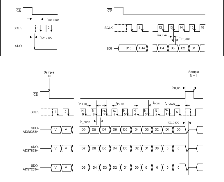 Figure 1. Serial Interface Timing Diagram
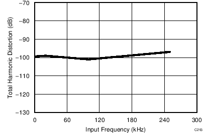
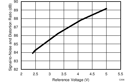
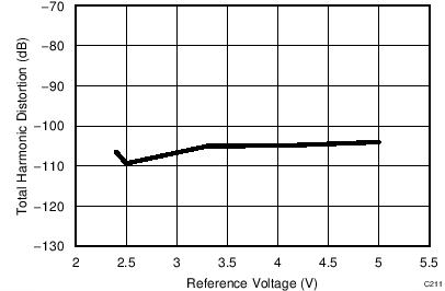
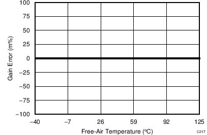
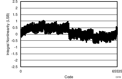
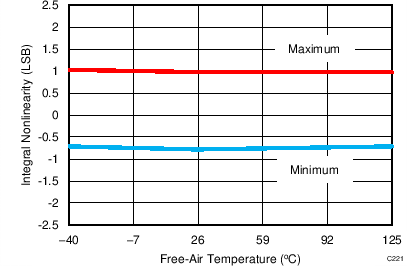
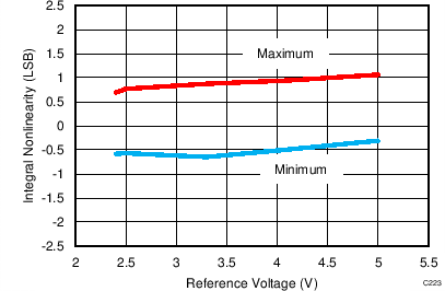
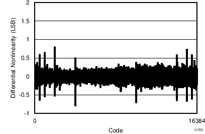
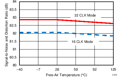
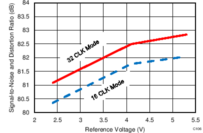
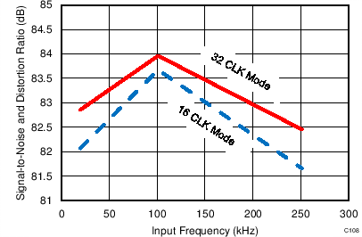
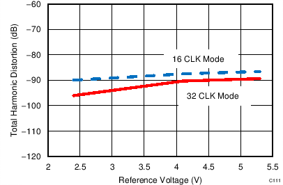
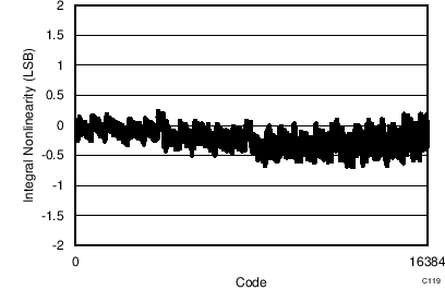
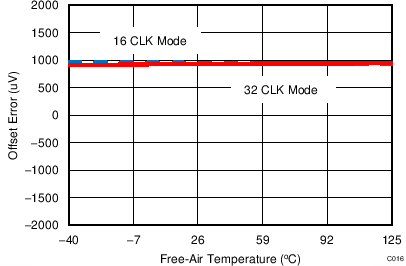
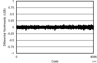
7.11 Typical Characteristics: ADS8353
At TA = 25°C, AVDD = 5 V, DVDD = 3.3 V, VREF = 2.5 V (internal), and fDATA = 600 kSPS, unless otherwise noted.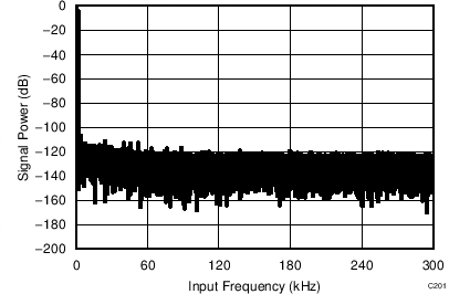
| fIN = 2 kHz | SNR = 84.2 dB | THD = -101.3 dB |
| fIN = 2 kHz |
| fIN = 2 kHz |
| VREF = 5 V |
| fIN = 2 kHz |
| VREF = 5 V |
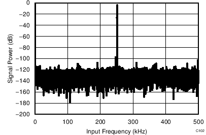
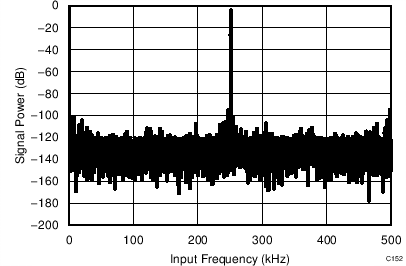
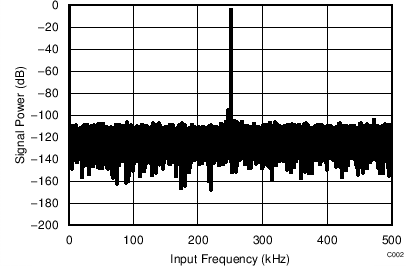
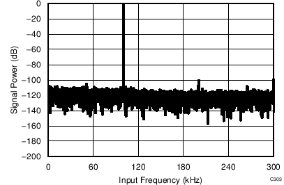
| fIN = 100 kHz | SNR = 80.8 dB | THD = -99.1 dB |
| fIN = 2 kHz |
| fIN = 2 kHz |
| VREF = 5 V |
| fIN = 2 kHz |
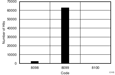
| 65536 data points | VIN-DIFF = 0 V |
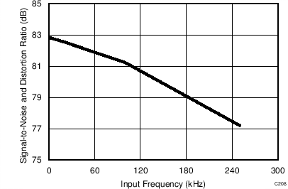
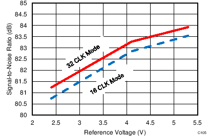
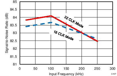
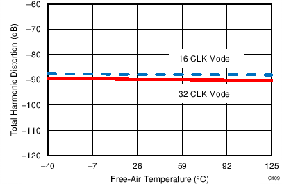
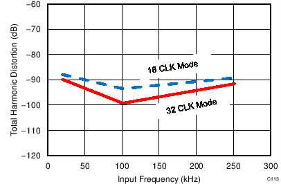
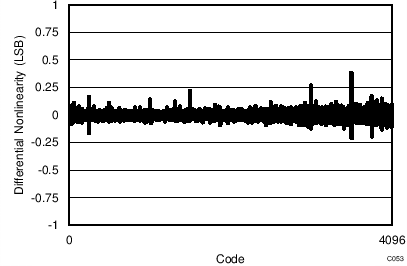
7.12 Typical Characteristics: ADS7853
At TA = 25°C, AVDD = 5 V, DVDD = 3.3 V, VREF = 2.5 V (internal), and fDATA = 1 MSPS, unless otherwise noted.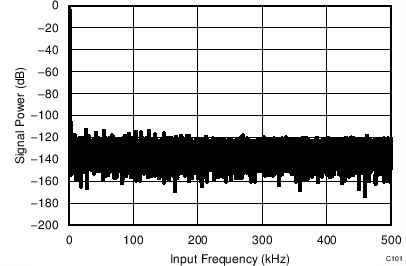
| fIN = 2 kHz | SNR = 81.1 dB | THD = –94.2 dB |
| 16-CLK interface |
| fIN = 2 kHz | SNR = 81.9 dB | THD = –98.1 dB |
| 32-CLK interface |
| fIN = 2 kHz |
| fIN = 2 kHz |
| VREF = 5 V |
| fIN = 2 kHz |
| VREF = 5 V |
| 16-CLK interface |
| 16-CLK interface | 65536 data points | VIN-DIFF = 0 V |
| 16-CLK interface |
| 32-CLK interface |
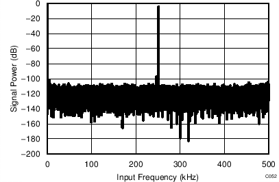
| fIN = 250 kHz | SNR = 80.2 dB | THD = –90.4 dB |
| 16-CLK interface |
| fIN = 250 kHz | SNR = 80.8 dB | THD = –92.1 dB |
| 32-CLK interface |
| fIN = 2 kHz |
| fIN = 2 kHz |
| VREF = 5 V |
| fIN = 2 kHz |
| 32-CLK interface |
| 32-CLK interface | 65536 data points | VIN-DIFF = 0 V |
| 16-CLK interface |
| 32-CLK interface |
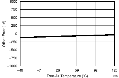
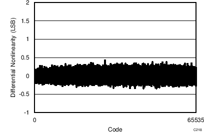
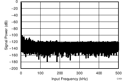
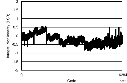
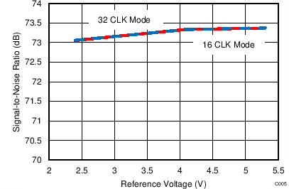
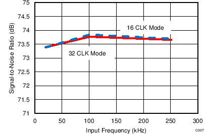
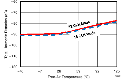
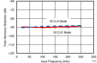
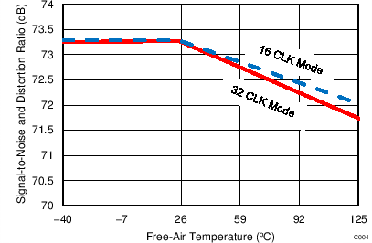
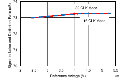
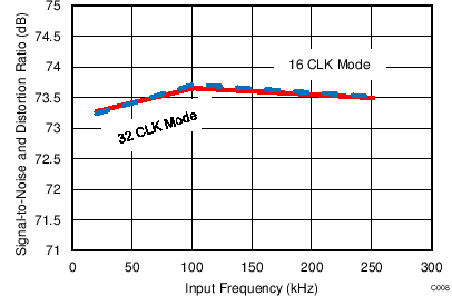
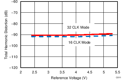
7.13 Typical Characteristics: ADS7253
At TA = 25°C, AVDD = 5 V, DVDD = 3.3 V, VREF = 2.5 V (internal), and fDATA = 1 MSPS, unless otherwise noted.
| fIN = 2 kHz | SNR = 73.2 dB | THD = –90.5 dB |
| 16-CLK interface |
| fIN = 2 kHz | SNR = 73.6 dB | THD = –91.6 dB |
| 32-CLK interface |
| fIN = 2 kHz |
| fIN = 2 kHz |
| VREF = 5 V |
| fIN = 2 kHz |
| VREF = 5 V |
| 16-CLK interface |
| 16-CLK interface | 65536 data points | VIN-DIFF = 0 V |
| 16-CLK interface |
| 32-CLK interface |
| fIN = 250 kHz | SNR = 73.1 dB | THD = –90.1 dB |
| 16-CLK interface |
| fIN = 250 kHz | SNR = 73.4 dB | THD = –90.6 dB |
| 32-CLK interface |
| fIN = 2 kHz |
| fIN = 2 kHz |
| VREF = 5 V |
| fIN = 2 kHz |
| 32-CLK interface |
| 32-CLK interface | 65536 data points | VIN-DIFF = 0 V |
| 16-CLK interface |
| 32-CLK interface |
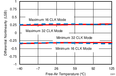
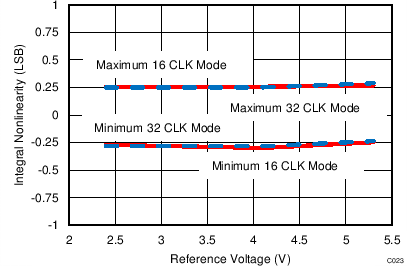
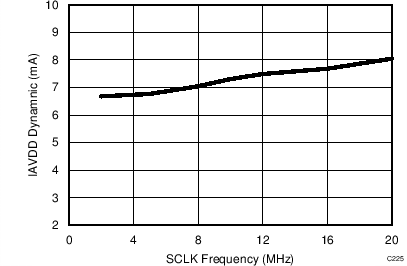
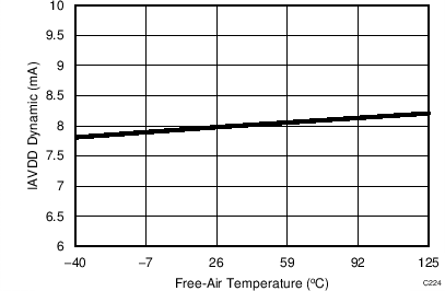
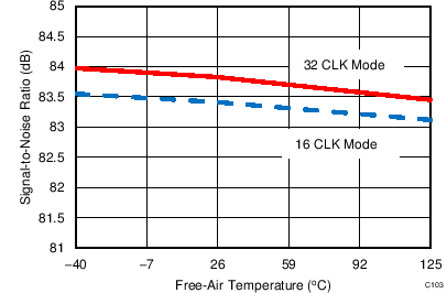
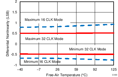
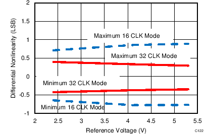
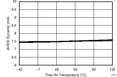
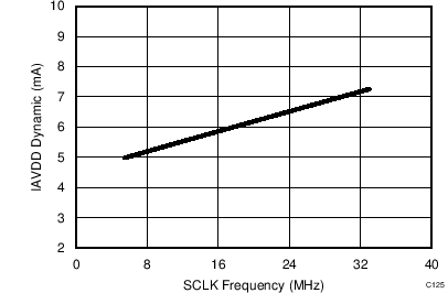
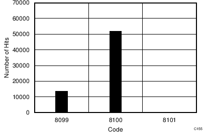
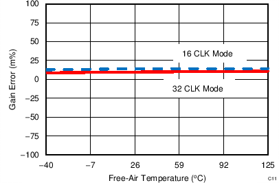
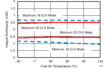
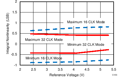
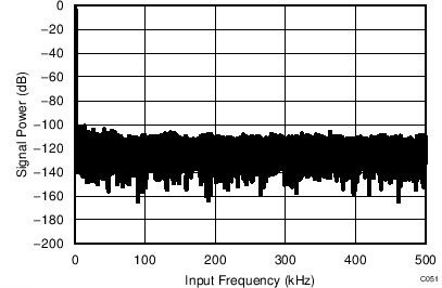
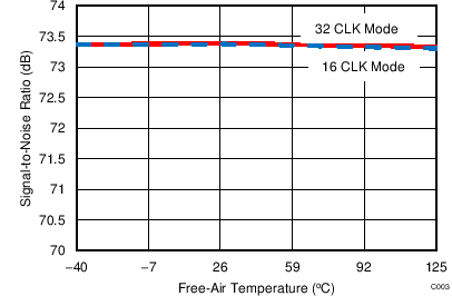
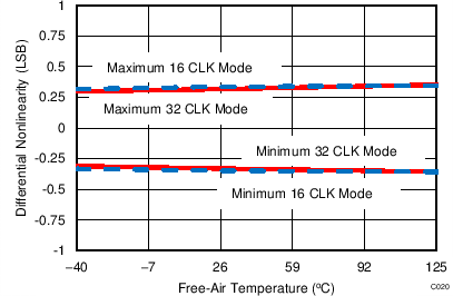
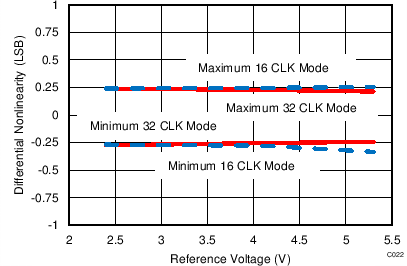
7.14 Typical Characteristics: Common to ADS8353, ADS7853, and ADS7253
At TA = 25°C, AVDD = 5 V, DVDD = 3.3 V, VREF = 2.5 V (internal), and fDATA = maximum, unless otherwise noted.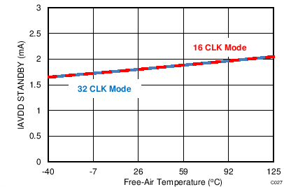
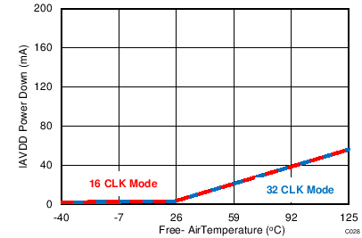
| ROUT = 0.67 Ω |
8 Detailed Description
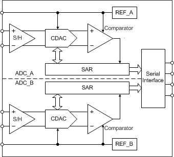
8.1 Overview
These devices belong to a family of pin-compatible, dual, high-speed, simultaneous-sampling, analog-to-digital converters (ADCs). The ADS8353, ADS7853, and ADS7253 support single-ended and pseudo-differential input signals. The devices provide a simple, serial interface to the host controller and operate over a wide range of analog and digital power supplies.
These devices have two independently programmable internal references to achieve system-level gain error correction. The Functional Block Diagram section provides a functional block diagram of the device.
8.2 Functional Block Diagram
8.3 Feature Description
8.3.1 Reference
The device has two simultaneous sampling ADCs (ADC_A and ADC_B). ADC_A and ADC_B operate with reference voltages VREF_A and VREF_B present on the REFIO_A and REFIO_B pins, respectively. The REFIO_A and REFIO_B pins should be decoupled with the REFGND_A and REFGND_B pins, respectively, with 10-µF decoupling capacitors.
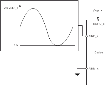
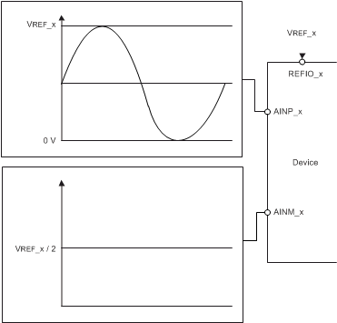
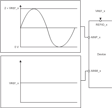
The device supports operation either with an internal or external reference source, as shown in Figure 84. The reference voltage source is determined by setting bit 6 of the configuration register (CFR.B6). Note that this bit is common to ADC_A and ADC_B.
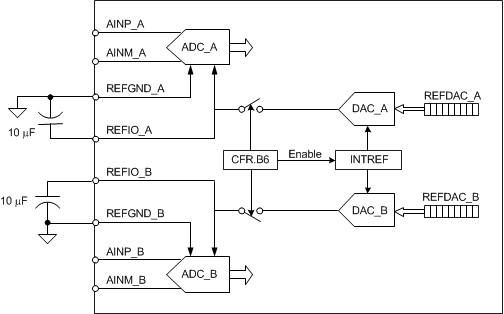 Figure 84. Reference Configurations and Connections
When CFR.B6 is 0, the device shuts down the internal reference source (INTREF) and ADC_A and ADC_B operate on external reference voltages provided by the user on the REFIO_A and REFIO_B pins, respectively.
When CFR.B6 is 1, the device operates with the internal reference source (INTREF) connected to REFIO_A and REFIO_B via DAC_A and DAC_B, respectively. In this configuration, VREF_A and VREF_B can be changed independently by writing to the respective user-programmable registers, REFDAC_A and REFDAC_B, respectively. Refer to the REFDAC Registers (REFDAC_A and REFDAC_B) section for more details.
8.3.2 Analog Inputs
The ADS8353, ADS7853, and ADS7253 support single-ended or pseudo-differential analog inputs on both ADC channels. These inputs are sampled and converted simultaneously by the two ADCs, ADC_A and ADC_B. ADC_A samples and converts (VAINP_A – VAINM_A), and ADC_B samples and converts (VAINP_B – VAINM_B).
Figure 85a and Figure 85b show equivalent circuits for the ADC_A and ADC_B analog input pins, respectively. Series resistance, RS, represents the on-state sampling switch resistance (typically 50 Ω) and CSAMPLE is the device sampling capacitor (typically 40 pF).
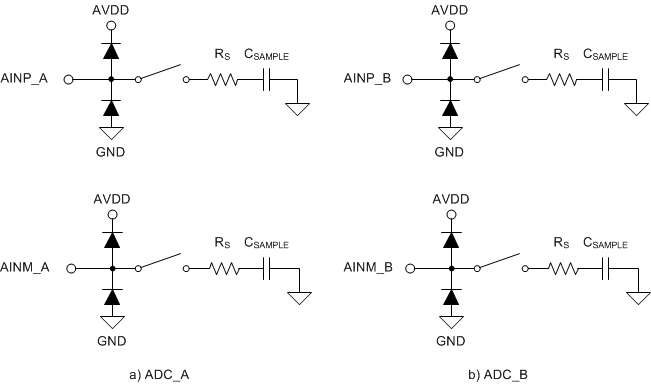 Figure 85. Equivalent Circuit for the Analog Input Pins
8.3.2.1 Analog Input: Full-Scale Range Selection
The full-scale range (FSR) supported at the analog inputs of the device is programmable with bit B9 of the configuration register (CFR.B9). This bit is common for both ADCs (ADC_A and ADC_B). The FSR is given by Equation 1 and Equation 2 :
where
- VREF_A and VREF_B are the reference voltages going to ADC_A and ADC_B, respectively (as described in the Reference section).
Therefore, with appropriate settings of the REFDAC_A and REFDAC_B registers, CFR.B7, and CFR.B9, the maximum dynamic range of the ADC can be used.
Note that while using CFR.B9 set to 1, care must be taken so that the ADC analog supply (AVDD) is as in Equation 3 and Equation 4:
8.3.2.2 Analog Input: Single-Ended and Pseudo-Differential Configurations
The ADS8353, ADS7853, and ADS7253 can support single-ended or pseudo-differential input configurations.
For supporting single-ended inputs, B7 in the configuration register (CFR.B7) must be set to 0 (CFR.B7 = 0) and AINM_A and AINM_B must be externally connected to GND.
For supporting pseudo-differential inputs, CFR.B7 must be set to 1 (CFR.B7 = 1) and AINM_A and AINM_B must be externally connected to FSR_ADC_A / 2 and FSR_ADC_B / 2, respectively. Note that CFR.B7 is common to both ADCs.
The CFR.B9 and CFR.B7 settings can be combined to select the desired input configuration, as shown in Table 1.
Table 1. Input Configurations
| INPUT RANGE SELECTION | AINM SELECTION | CONNECTION DIAGRAM |
|---|---|---|
| CFR.B9 = 0 (FSR_ADC_A = 0 to VREF_A) (FSR_ADC_B = 0 to VREF_B) |
CFR.B7 = 0 (AINM_A = GND) (AINM_B = GND) |
 |
| CFR.B9 = 1 (FSR_ADC_A = 0 to 2 x VREF_A) (FSR_ADC_B = 0 to 2 x VREF_B) |
CFR.B7 = 0 (AINM_A = GND) (AINM_B = GND) |
 |
| CFR.B9 = 0 (FSR_ADC_A = VREF_A) (FSR_ADC_B = VREF_B) |
CFR.B7 = 1 (AINM_A = VREF_A/2) (AINM_B = VREF_B/2) |
 |
| CFR.B9 = 1 (FSR_ADC_A = 2 x VREF_A) (FSR_ADC_B = 2 x VREF_B) |
CFR.B7 = 1 (AINM_A = VREF_A) (AINM_B = VREF_B) |
 |
8.3.3 Transfer Function
The device supports two input configurations:
- Single-ended inputs, CFR.B7 = 0 (default), or
- Pseudo-differential inputs, CFR.B7 = 1.
The device also supports two output data formats:
- Straight binary output, CFR.B4 = 0 (default), or
- Twos compliment output, CFR.B4 = 1.
Device resolution is calculated by Equation 5:
where
- N = 16 (ADS8353), 14 (ADS7853), or 12 (ADS7253) and
- FSR_ADC_x is the full-scale input range of the ADC (refer to the Analog Input section for more details)
Table 2 and Table 3 show the different input voltages and the corresponding output codes from the device.
Table 2. Transfer Characteristics for Straight Binary Output (CFR.B4 = 0, Default)
| INPUT CONFIGURATION | INPUT VOLTAGE | OUTPUT CODE (Hex) | |||||
|---|---|---|---|---|---|---|---|
| STRAIGHT BINARY (CFR.B4 = 0, Default) | |||||||
| AINP_x | AINM_x | AINP_x - AINM_x | CODE | ADS8353 | ADS7853 | ADS7253 | |
| Single-ended (CFR.B7 = 0, default) |
≤ 1 LSB | 0 | ≤ 1 LSB | ZC | 0000 | 0000 | 000 |
| FSR_ADC_x / 2 | FSR_ADC_x / 2 | MC | 7FFF | 1FFF | 7FF | ||
| ≥ FSR_ADC_x – 1 LSB | ≥ FSR_ADC_x – 1 LSB | FSC | FFFF | 3FFF | FFF | ||
| Pseudo-differential (CFR.B7 = 1) |
≤ 1 LSB | FSR_ADC_x / 2 | ≤ –FSR_ADC_x / 2 + 1 LSB | ZC | 0000 | 0000 | 000 |
| FSR_ADC_x / 2 | 0 | MC | 7FFF | 1FFF | 7FF | ||
| ≥ FSR_ADC_x – 1 LSB | ≥ FSR_ADC_x / 2 – 1 LSB | FSC | FFFF | 3FFF | FFF | ||
Table 3. Transfer Characteristics for Twos Compliment Output (CFR.B4 = 1)
| INPUT CONFIGURATION | INPUT VOLTAGE | OUTPUT CODE (Hex) | |||||
|---|---|---|---|---|---|---|---|
| TWOS COMPLIMENT (CFR.B4 = 1) | |||||||
| AINP_x | AINM_x | AINP_x - AINM_x | CODE | ADS8353 | ADS7853 | ADS7253 | |
| Single-ended (CFR.B7 = 0, default) |
≤ 1 LSB | 0 | ≤ 1 LSB | NFSC | 8000 | 2000 | 800 |
| FSR_ADC_x / 2 | FSR_ADC_x / 2 | MC | 0000 | 0000 | 000 | ||
| ≥ FSR_ADC_x – 1 LSB | ≥ FSR_ADC_x – 1 LSB | PFSC | 7FFF | 1FFF | 7FF | ||
| Pseudo-differential (CFR.B7 = 1) |
≤ 1 LSB | FSR_ADC_x / 2 | ≤ –FSR_ADC_x / 2 + 1 LSB | NFSC | 8000 | 2000 | 800 |
| FSR_ADC_x / 2 | 0 | MC | 0000 | 0000 | 000 | ||
| ≥ FSR_ADC_x – 1 LSB | ≥ FSR_ADC_x / 2 – 1 LSB | PFSC | 7FFF | 1FFF | 7FF | ||
Figure 86 shows the ideal device transfer characteristics for the single-ended analog input.
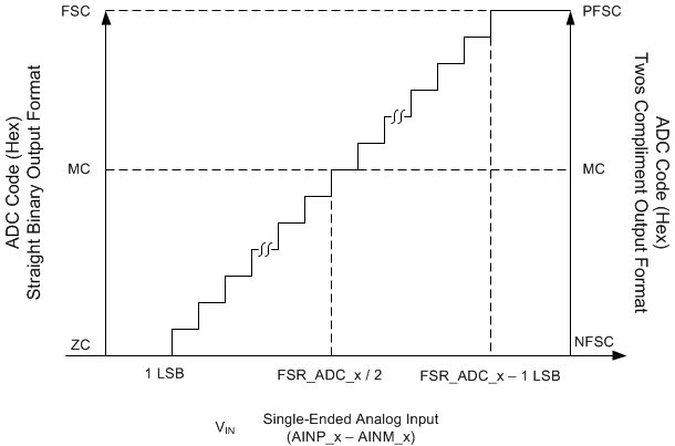 Figure 86. Ideal Transfer Characteristics for a Single-Ended Analog Input
Figure 87 shows the ideal device transfer characteristics for the pseudo-differential analog input.
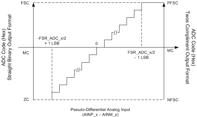 Figure 87. Ideal Transfer Characteristics for a Pseudo-Differential Analog Input
8.4 Device Functional Modes
The device provides three user-programmable registers: the configuration register (CFR), the REFDAC_A register, and the REFDAC_B register. These registers support write (refer to the Write to User Programmable Registers section) and readback (refer to the Reading User-Programmable Registers section) operations and allow the user to customize ADC behavior for specific application requirements.
The device supports four interface modes (refer to the Conversion Data Read section), two low-power modes (refer to the Low-Power Modes section), and short-cycling/reconversion feature (refer to the Frame Abort, Reconversion, or Short-Cycling section).
8.5 Register Maps and Serial Interface
8.5.1 Serial Interface
The device uses the serial clock (SCLK) for synchronizing data transfers in and out of the device.
The CS signal defines one conversion and serial transfer frame. A frame starts with a CS falling edge and ends with a CS rising edge. Between the start and end of the frame, a minimum of N SCLK falling edges must be provided to validate the read or write operation. As shown in Table 4, N depends upon the interface mode used to read the conversion result. When N SCLK falling edges are provided, the write operation attempted in the frame is validated and the internal user-programmable registers are updated on the subsequent CS rising edge. This CS rising edge also ends the frame.
Table 4. SCLK Falling Edges for a Valid Write Operation
| INTERFACE MODE | MINIMUM SCLK FALLING EDGES REQUIRED TO VALIDATE WRITE OPERATION N |
|---|---|
| 32-CLK, dual-SDO mode (default). See the 32-CLK, Dual-SDO Mode section. | 32 |
| 32-CLK, single-SDO mode. See the 32-CLK, Single-SDO Mode section. | 48 |
| 16-CLK, dual-SDO mode. See the 16-CLK, Dual-SDO Mode section. | 16 |
| 16-CLK, single SDO mode. See the 16-CLK, Single SDO Mode section. | 32 |
If CS is brought high before providing N SCLK falling edges, the write operation attempted in the frame is not valid. Refer to the Frame Abort, Reconversion, or Short-Cycling section for more details.
8.5.2 Write to User Programmable Registers
The device features three user-programmable registers: the configuration register (CFR), the REFDAC_A register, and the REFDAC_B register. These registers can be written with the device SDI pin. The first 16 bits of data on SDI are latched into the device on the first 16 SCLK falling edges. However, the new configuration takes effect only when the read or write operation is validated. If these registers are not required to update, SDI must remain low during the respective frames.
The first four SDI data bits (B[15:12]) determine what operation is performed (that is, either a read or write operation or no operation), which register address the operation uses, and the function of the next 12 SDI data bits (B[11:0]). Table 5 lists the various combinations supported for B[15:12].
Table 5. Data Write Operation
| B15 | B14 | B13 | B12 | OPERATION | FUNCTION OF BITS B[11:0] |
|---|---|---|---|---|---|
| 0 | 0 | 0 | 0 | No operation is performed | These bits are ignored |
| 0 | 0 | 0 | 1 | REFDAC_A read | 000h; see the Reading User-Programmable Registers section |
| 0 | 0 | 1 | 0 | REFDAC_B read | 000h; see the Reading User-Programmable Registers section |
| 0 | 0 | 1 | 1 | CFR read | 000h; see the Reading User-Programmable Registers section |
| 1 | 0 | 0 | 0 | CFR write | See the Configuration Register (CFR) section |
| 1 | 0 | 0 | 1 | REFDAC_A write | See the REFDAC_A section |
| 1 | 0 | 1 | 0 | REFDAC_B write | See the REFDAC_B section |
| 1 | 0 | 1 | 1 | No operation is performed | These bits are ignored |
| X | 1 | X | X | No operation is performed | These bits are ignored |
8.5.2.1 Configuration Register (CFR)
The device operation configuration is controlled by the configuration register (CFR) status. Data written into the CFR in a valid frame (F) determine the device configuration for frame (F+1). The bit functions are outlined in Figure 88. On power-up, all bits in the CFR default to 0.
| 15 | 14 | 13 | 12 | 11 | 10 | 9 | 8 |
| WRITE/READ | 0 | ADDR1 | ADDR0 | RD_CLK_ MODE |
RD_DATA_ LINES |
INPUT_RANGE | 0 |
| 7 | 6 | 5 | 4 | 3 | 2 | 1 | 0 |
| INM_SEL | REF_SEL | STANDBY | RD_DATA_ FORMAT |
0 | 0 | 0 | 0 |
Table 6. Configuration Register (CFR) Field Descriptions
| Bit | Field | Type | Reset | Description |
|---|---|---|---|---|
| 15 | WRITE/READ | W | 0h | These bits select the user-programmable register. 1000 = Select this combination to write to the CFR register and to enable bits 11:0 |
| 14 | 0 | R/W | 0h | |
| 13 | ADDR1 | R/W | 0h | |
| 12 | ADDR0 | R/W | 0h | |
| 11 | RD_CLK_MODE | R/W | 0h | This bit provides clock mode selection for the serial interface. 0 = Selects 32-CLK mode (default) 1 = Selects 16-CLK mode (Note that the ADS8353 only supports 32-CLK mode. This bit is ignored for the ADS8353.) |
| 10 | RD_DATA_LINES | R/W | 0h | This bit provides data line selection for the serial interface. 0 = Use SDO_A to output ADC_A data and SDO_B to output of ADC_B data (default) 1 = Use only SDO_A to output of ADC_A data followed by ADC_B data |
| 9 | INPUT_RANGE | R/W | 0h | This bit selects the maximum input range for the ADC as a function of the reference voltage provided to the ADC. See the Analog Inputs section for more details. 0 = FSR equals VREF 1 = FSR equals 2 × VREF |
| 8 | 0 | R/W | 0h | This bit must be set to 0 (default) |
| 7 | INM_SEL | R/W | 0h | This bit selects the voltage to be externally connected to the INM pin. 0 = INM must be externally connected to the GND potential (default) 1 = INM must be externally connected to the FSR_ADC_x / 2 potential |
| 6 | REF_SEL | R/W | 0h | This bit selects the ADC reference voltage source. Refer to the Reference section for more details. 0 = Use external reference (default) 1 = Use internal reference |
| 5 | STANDBY | W | 0h | This bit is used by the device to enter or exit STANDBY mode. Refer to the STANDBY Mode section for more details. |
| 4 | RD_DATA_FORMAT | R/W | 0h | This bit selects the output data format. 0 = Output is in straight binary format (default) 1 = Output is in twos compliment format |
| 3:0 | 0 | R/W | 0h | These bits must be set to 0 (default) |
8.5.2.2 REFDAC Registers (REFDAC_A and REFDAC_B)
The REFDAC registers, bit functions, and resolution information are described in this section.
| 15 | 14 | 13 | 12 | 11 | 10 | 9 | 8 |
| WRITE/READ | 0 | ADDR1 | ADDR0 | D8 | D7 | D6 | D5 |
| 7 | 6 | 5 | 4 | 3 | 2 | 1 | 0 |
| D4 | D3 | D2 | D1 | D0 | 0 | 0 | 0 |
Table 7. REFDAC Registers Field Descriptions
| Bit | Field | Type | Reset | Description |
|---|---|---|---|---|
| 15 | WRITE/READ | W | 0h | These bits select the configurable register address. 1001 = Select this combination to write to the REFDAC_A register 1010 = Select this combination to write to the REFDAC_B register |
| 14 | 0 | R/W | 0h | |
| 13 | ADDR1 | R/W | 0h | |
| 12 | ADDR0 | R/W | 0h | |
| 11:3 | D[8:0] | R/W | 0h | Data to program the individual DAC output voltage. Note: These bits are valid only for bits 15:12 = 1001 or bits 15:12 = 1010. Table 8 shows the relationship between the REFDAC_x programmed value and the DAC_x output voltage. |
| 2:0 | 0 | R/W | 0h | This bit must be set to 0 (default) |
Table 8. REFDAC Settings
| REFDAC_x VALUE (Bits 11:3 in Hex) | B[2:0] | Typical DAC_x OUPTUT VOLTAGE (V)(1) | |||
|---|---|---|---|---|---|
| 1FF (default) | 000 | 2.5000 | |||
| 1FE | 000 | 2.4989 | |||
| 1FD | 000 | 2.4978 | |||
| — | — | — | |||
| 1D7 | 000 | 2.45 | |||
| — | — | — | |||
| 1AE | 000 | 2.40 | |||
| — | — | — | |||
| 186 | 000 | 2.35 | |||
| — | — | — | |||
| 15D | 000 | 2.30 | |||
| — | — | — | |||
| 134 | 000 | 2.25 | |||
| — | — | — | |||
| 10C | 000 | 2.20 | |||
| — | — | — | |||
| 0E3 | 000 | 2.15 | |||
| — | — | — | |||
| 0BA | 000 | 2.10 | |||
| — | — | — | |||
| 091 | 000 | 2.05 | |||
| — | — | — | |||
| 069 | 000 | 2.00 | |||
| — | — | — | |||
| 064 to 000 | 000 | Do not use | |||
8.5.3 Data Read Operation
The device supports two types of read operations: reading user-programmable registers and reading conversion results.
8.5.3.1 Reading User-Programmable Registers
The device supports a readback option for all user-programmable registers: CFR, REFDAC_A, and REFDAC_B. Figure 90 shows a detailed timing diagram for this operation.
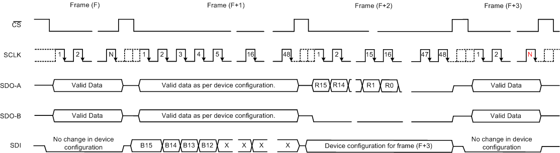
To readback the user-programmable register settings, the appropriate control word should be transmitted to the device during frame (F+1), as shown in Table 9. Frame (F+1) must have at least 48 SCLK falling edges.
Table 9. Control Word to Readback User-Programmable Registers
| USER-PROGRAMMABLE REGISTER | CONTROL WORD TO BE PROGRAMMED IN FRAME (F+1) | |
|---|---|---|
| B[15:12] (Binary) | B[11:0] (Hex) | |
| CFR | 0011b | 000h |
| REFDAC_A | 0001b | 000h |
| REFDAC_B | 0010b | 000h |
Frame (F+2) must have at least 48 SCLK falling edges. During frame (F+2), SDO_A outputs the contents of the selected user-programmable register on the first 16 SCLK falling edges (as shown in Table 10) and then outputs 0s for any subsequent SCLK falling edges. The SDO_B pin outputs 0s for all the SCLK falling edges.
Table 10. Register Data Read Back
| USER-PROGRAMMABLE REGISTER | DATA READ ON SDO-A IN FRAME (F+2) | |||||||||
|---|---|---|---|---|---|---|---|---|---|---|
| R15 | R14 | R13 | R12 | R11 | — | R3 | R2 | R1 | R0 | |
| CFR | 0 | 0 | 1 | 1 | CFG.B11 | — | CFG.B3 | CFG.B2 | CFG.B1 | CFG.B0 |
| REFDAC_A | 0 | 0 | 0 | 1 | REFDAC_A.D8 | — | REFDAC_A.D0 | 0 | 0 | 0 |
| REFDAC_B | 0 | 0 | 1 | 0 | REFDAC_B.D8 | — | REFDAC_B.D0 | 0 | 0 | 0 |
Register settings programmed during frame (F+2) determine the device configuration in frame (F+3).
8.5.3.2 Conversion Data Read
The device provides four different interface modes to the user for reading the conversion result. These modes offer flexible hardware connections and firmware programming. Table 11 shows how to select one of the four interface modes.
Table 11. Interface Mode Selection
| CFR.B11 | CFR.B10 | INTERFACE MODE | MINIMUM SCLK FALLING EDGES REQUIRED TO VALIDATE WRITE OPERATION N |
|---|---|---|---|
| 0 | 0 | 32-CLK, dual-SDO mode (default) | 32 |
| 0 | 1 | 32-CLK, single-SDO mode | 48 |
| 1 | 0 | 16-CLK, dual-SDO mode | 16 |
| 1 | 1 | 16-CLK, single SDO mode | 32 |
In the 32-CLK interface modes, the device uses an internal clock to convert the sampled analog signal. The conversion is completed during the first 16 periods of SCLK and the conversion result can be read on the subsequent SCLK falling edges. All devices in the family (that is, ADS8353, ADS7853, and ADS7253) support the 32-CLK interface modes.
In addition to the 32-CLK interface modes, the ADS7853 and ADS7253 also support the 16-CLK interface modes. By using the 16-CLK interface modes, the same throughput can be achieved at much lower SCLK speeds.
The following sections detail the various interface modes supported by the device.
8.5.3.2.1 32-CLK, Dual-SDO Mode (CFR.B11 = 0, CFR.B10 = 0, Default)
The 32-CLK, dual-SDO mode is the default mode supported by all devices. This mode can also be selected by writing CFR.B11 = 0 and CFR.B10 = 0.
In this mode, the SDO_A pin outputs the ADC_A conversion result and the SDO_B pin outputs the ADC_B conversion result. Figure 91 shows a detailed timing diagram for this mode.
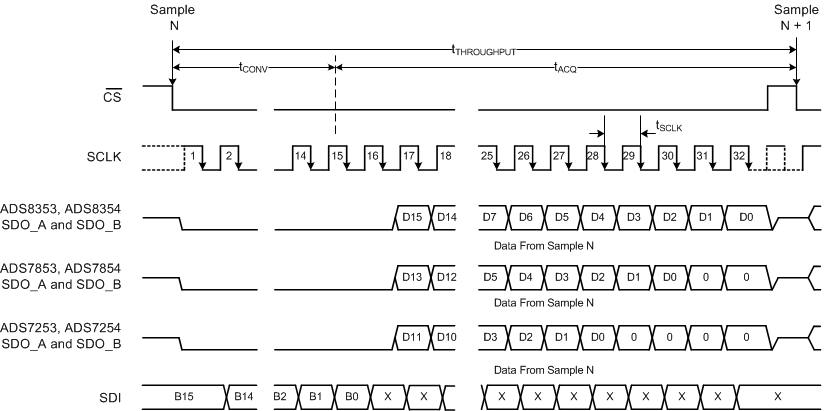 Figure 91. 32-CLK, Dual-SDO Mode Timing Diagram
A CS falling edge brings the serial data bus out of 3-state and also outputs a 0 on the SDO_A and SDO_B pins. The device converts the sampled analog input during the conversion time (tCONV). SDO_A and SDO_B read 0 during this period. After completing the conversion process, the sample-and-hold circuit returns to sample mode. The device outputs the MSBs of ADC_A and ADC_B on SDO_A and SDO_B pins, respectively, on the 16th SCLK falling edge. The subsequent SCLK falling edges are used to shift out the rest of the bits of the conversion result, as shown in Table 12.
Table 12. Data Launch Edge
| DEVICE | PINS | LAUNCH EDGE | ||||||||||||
|---|---|---|---|---|---|---|---|---|---|---|---|---|---|---|
| CS | SCLK | CS | ||||||||||||
| ↓ | ↓1 | — | ↓15 | ↓16 | — | ↓27 | ↓28 | ↓29 | ↓30 | ↓31 | ↓32 ... | ↑ | ||
| ADS8353 | SDO-A | 0 | 0 | — | 0 | D15_A | — | D4_A | D3_A | D2_A | D1_A | D0_A | 0 ... | Hi-Z |
| SDO-B | 0 | 0 | — | 0 | D15_B | — | D4_B | D3_B | D2_B | D1_B | D0_B | 0 ... | Hi-Z | |
| ADS7853 | SDO-A | 0 | 0 | — | 0 | D13_A | — | D2_A | D1_A | D0_A | 0 | 0 | 0 ... | Hi-Z |
| SDO-B | 0 | 0 | — | 0 | D13_B | — | D2_B | D1_B | D0_B | 0 | 0 | 0 ... | Hi-Z | |
| ADS7253 | SDO-A | 0 | 0 | — | 0 | D11_A | — | D0_A | 0 | 0 | 0 | 0 | 0 ... | Hi-Z |
| SDO-B | 0 | 0 | — | 0 | D11_B | — | D0_B | 0 | 0 | 0 | 0 | 0 ... | Hi-Z | |
In this mode, at least 32 SCLK falling edges must be given to validate the read or write frame. A CS rising edge ends the frame and puts the serial bus into 3-state.
Refer to Table 13 for timing specifications specific to this serial interface mode.
Table 13. 32-CLK, Dual-SDO Interface Specific Timing
| PARAMETER | TEST CONDITIONS | MIN | TYP | MAX | UNIT | |
|---|---|---|---|---|---|---|
| TIMING REQUIREMENTS | ||||||
| tCLK | CLOCK period | ADS8353 | 50 | ns | ||
| ADS7853 | 29.4 | ns | ||||
| ADS7253 | 29.4 | ns | ||||
| tACQ | Acquisition time | 33 × tCLK – tCONV | ns | |||
| TIMING SPECIFICATIONS | ||||||
| tCONV | Conversion time | ADS8353 | 730 | ns | ||
| ADS7853 | 450 | ns | ||||
| ADS7253 | 450 | ns | ||||
8.5.3.2.2 32-CLK, Single-SDO Mode (CFR.B11 = 0, CFR.B10 = 1)
The 32-CLK, single-SDO mode provides the option of using only one SDO pin (SDO_A) to read conversion results from both ADCs (ADC_A and ADC_B). SDO_B remains in 3-state and can be treated as a no connect (NC) pin.
This mode can be selected by writing CFR.B11 = 0 and CFR.B10 = 1. Figure 92 shows a detailed timing diagram for this mode.
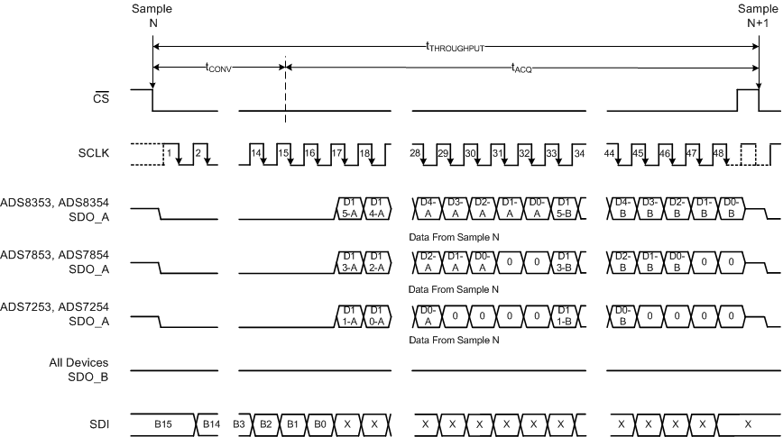 Figure 92. 32-CLK, Single-SDO Mode Timing Diagram
A CS falling edge brings the serial data bus out of 3-state and also outputs a 0 on the SDO_A pin. The device converts the sampled analog input during the conversion time (tCONV). SDO_A reads 0 during this period. After competing the conversion process, the sample-and-hold circuit goes back into sample mode. The device outputs the MSB of ADC_A on the SDO_A pin on the 16th SCLK falling edge. The subsequent SCLK falling edges are used to shift out the conversion result of ADC_A followed by the conversion result of ADC_B on the SDO_A pin, as shown in Table 14.
Table 14. Data Launch Edge
| DEVICE | PIN | LAUNCH EDGE | |||||||||||||||||||
|---|---|---|---|---|---|---|---|---|---|---|---|---|---|---|---|---|---|---|---|---|---|
| CS | SCLK | CS | |||||||||||||||||||
| ↓ | ↓1 | — | ↓15 | ↓16 | — | ↓27 | ↓28 | ↓29 | ↓30 | ↓31 | ↓32 | — | ↓43 | ↓44 | ↓45 | ↓46 | ↓47 | ↓48 ... | ↑ | ||
| ADS8353 | SDO-A | 0 | 0 | — | 0 | D15_A | — | D4_A | D3_A | D2_A | D1_A | D0_A | D15_B | — | D4_B | D3_B | D2_B | D1_B | D0_B | 0 ... | Hi-Z |
| ADS7853 | SDO-A | 0 | 0 | — | 0 | D13_A | — | D2_A | D1_A | D0_A | 0 | 0 | 0 | — | D2_B | D1_B | D0_B | 0 | 0 | 0 ... | Hi-Z |
| ADS7253 | SDO-A | 0 | 0 | — | 0 | D11_A | — | D0_A | 0 | 0 | 0 | 0 | 0 | — | D0_B | 0 | 0 | 0 | 0 | 0 ... | Hi-Z |
In this mode, at least 48 SCLK falling edges must be given to validate the read or write frame. A CS rising edge ends the frame and puts the serial bus into 3-state.
Refer to Table 15 for timing specifications specific to this serial interface mode.
Table 15. 32-CLK, Single-SDO Interface Specific Timing
| PARAMETER | TEST CONDITIONS | MIN | TYP | MAX | UNIT | |
|---|---|---|---|---|---|---|
| TIMING REQUIREMENTS | ||||||
| tCLK | CLOCK period | ADS8353 | 50 | ns | ||
| ADS7853 | 29.4 | ns | ||||
| ADS7253 | 29.4 | ns | ||||
| tACQ | Acquisition time | 49 × tCLK – tCONV | ns | |||
| TIMING SPECIFICATIONS | ||||||
| tCONV | Conversion time | ADS8353 | 730 | ns | ||
| ADS7853 | 450 | ns | ||||
| ADS7253 | 450 | ns | ||||
8.5.3.2.3 16-CLK, Dual-SDO Mode (CFR.B11 = 1, CFR.B10 = 0)
The 16-CLK, dual-SDO mode is designed to support the maximum throughput at lower SCLK frequencies. This interface mode is not supported by the ADS8353.
For the ADS7853 and ADS7253, this interface mode can be selected by writing CFR.B11 = 1 and CFR.B10 = 0. In this mode, the SDO_A pin outputs the ADC_A conversion result and the SDO_B pin outputs the ADC_B conversion result. Figure 93 shows a detailed timing diagram for this mode.
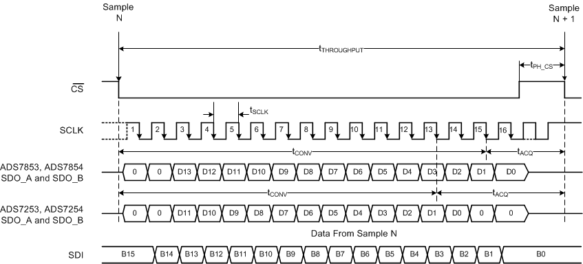 Figure 93. 16-CLK, Dual-SDO Mode Timing Diagram
A CS falling edge brings the serial data bus out of 3-state and also outputs a 0 on the SDO_A and SDO_B pins. The subsequent SCLK falling edges are used for conversion and for data transfer using the serial interface, as shown in Table 16.
The sample-and-hold circuit goes back into sample mode as soon as the conversion process is over.
Table 16. Data Launch Edge
| DEVICE | PINS | LAUNCH EDGE | ||||||||
|---|---|---|---|---|---|---|---|---|---|---|
| CS | SCLK | CS | ||||||||
| ↓ | ↓1 | ↓2 | — | ↓13 | ↓14 | ↓15 | ↓16 ... | ↑ | ||
| ADS7853 | SDO-A | 0 | 0 | D13_A | — | D2_A | D1_A | D0_A | 0 ... | Hi-Z |
| SDO-B | 0 | 0 | D13_B | — | D2_B | D1_B | D0_B | 0 ... | Hi-Z | |
| ADS7253 | SDO-A | 0 | 0 | D11_A | — | D0_A | 0 | 0 | 0 ... | Hi-Z |
| SDO-B | 0 | 0 | D11_B | — | D0_B | 0 | 0 | 0 ... | Hi-Z | |
In this mode, at least 16 SCLK falling edges must be given to validate the read or write frame. A CS rising edge ends the frame and puts the serial bus into 3-state.
Refer to Table 17 for timing specifications specific to this serial interface mode.
Table 17. 16-CLK, Dual-SDO Interface Specific Timing
| PARAMETER | TEST CONDITIONS | MIN | TYP | MAX | UNIT | |
|---|---|---|---|---|---|---|
| TIMING REQUIREMENTS | ||||||
| tCLK | CLOCK period | ADS7853 | 55.5 | ns | ||
| ADS7253 | 55.5 | ns | ||||
| tACQ | Acquisition time | ADS7853 | 4 × tCLK | ns | ||
| ADS7253 | 6 × tCLK | ns | ||||
| TIMING SPECIFICATIONS | ||||||
| tCONV | Conversion time | ADS7853 | 14 × tCLK | ns | ||
| ADS7253 | 12 × tCLK | ns | ||||
8.5.3.2.4 16-CLK, Single-SDO Mode (CFR.B11 = 1, CFR.B10 = 1)
The 16-CLK, single-SDO mode provides the option of using only one SDO pin (SDO_A) and a lower-speed clock to read the conversion results of both ADCs. This interface mode is not supported by the ADS8353.
For the ADS7853 and ADS7253, this mode can be selected by writing CFR.B11 = 1 and CFR.B10 = 1. The SDO_A pin is used to output the conversion results of both ADCs (ADC_A and ADC_B). SDO_B remains in 3-state and can be treated as a no connect (NC) pin. Figure 94 shows a detailed timing diagram for this mode.
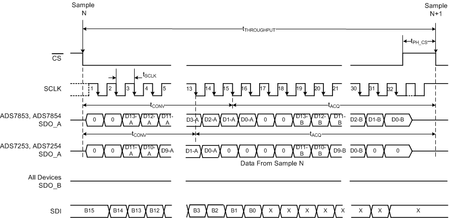 Figure 94. 16-CLK, Single-SDO Mode Timing Diagram
A CS falling edge brings the serial data bus out of 3-state and also outputs a 0 on the SDO_A pin. The subsequent SCLK falling edges are used for conversion and for data transfer using the serial interface, as shown in Table 18.
The sample-and-hold circuit goes back into sample mode as soon as the conversion process is over.
Table 18. Data Launch Edge
| DEVICE | PIN | LAUNCH EDGE | |||||||||||||||
|---|---|---|---|---|---|---|---|---|---|---|---|---|---|---|---|---|---|
| CS | SCLK | CS | |||||||||||||||
| ↓ | ↓1 | ↓2 | — | ↓13 | ↓14 | ↓15 | ↓16 | ↓17 | ↓18 | — | ↓29 | ↓30 | ↓31 | ↓32 ... | ↑ | ||
| ADS7853 | SDO-A | 0 | 0 | D13_A | — | D2_A | D1_A | D0_A | 0 | 0 | D13_B | — | D2_B | D1_B | D0_B | 0 ... | Hi-Z |
| ADS7253 | SDO-A | 0 | 0 | D11_A | — | D0_A | 0 | 0 | 0 | 0 | D11_B | — | D0_B | 0 | 0 | 0 ... | Hi-Z |
In this mode, at least 32 SCLK falling edges must be given to validate the read/write frame. A CS rising edge ends the frame and puts the serial bus into 3-state.
Refer to Table 19 for timing specifications specific to this serial interface mode.
Table 19. 16-CLK, Single-SDO Interface Specific Timing
| PARAMETER | TEST CONDITIONS | MIN | TYP | MAX | UNIT | |
|---|---|---|---|---|---|---|
| TIMING REQUIREMENTS | ||||||
| tCLK | CLOCK period | ADS7853 | 55.5 | ns | ||
| ADS7253 | 55.5 | ns | ||||
| tACQ | Acquisition time | ADS7853 | 19 × tCLK | ns | ||
| ADS7253 | 21 × tCLK | ns | ||||
| TIMING SPECIFICATIONS | ||||||
| tCONV | Conversion time | ADS7853 | 14 × tCLK | ns | ||
| ADS7253 | 12 × tCLK | ns | ||||
8.5.4 Low-Power Modes
In normal mode of operation, all internal circuits of the device are always powered up and the device is always ready to commence a new conversion. This mode enables the device to support the rated throughput. The device also supports two low-power modes to optimize the power consumption at lower throughputs: STANDBY mode and software power-down (SPD) mode.
8.5.4.1 STANDBY Mode
The device supports a STANDBY mode of operation where some of the internal circuits of the device are powered down. However, if bit 6 in configuration register is set to 1 (CFR.B6 = 1), then the internal reference is not powered down and the contents of the REFDAC_A and REFDAC_B registers are retained to enable faster power-up to a normal mode of operation.
As shown in Figure 95, a valid write operation in frame (F) to program the configuration register with B5 set to 1 (CFR.B5 = 1) places the device into a STANDBY mode of operation on the following CS rising edge. While in STANDBY mode, SDO_A and SDO_B output all 1s when CS is low and remain in 3-state when CS is high.
To remain in STANDBY mode, SDI must remain low in the subsequent frames.
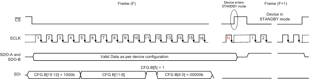
As shown in Figure 96, a valid write operation in frame (F+3) by writing the configuration register with B5 set to 0 (CFR.B5 = 0) brings the device out of STANDBY mode on the following CS rising edge. Frame (F+3) must have at least 48 SCLK falling edges.
After exiting the STANDBY mode, a delay of tPU_STDBY must elapse for the internal circuits to fully power-up and resume normal operation in frame (F+4). Device configuration for frame (F+4) is determined by the status of the CFR.B[11:6] bits programmed during frame (F+3).
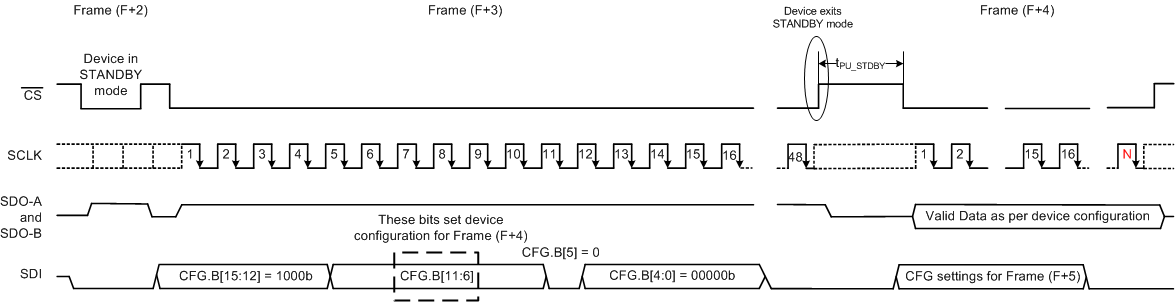
Refer to the Timing Characteristics: Serial Interface for timing specifications for this operating mode.
8.5.4.2 Software Power-Down (SPD) Mode
In software power-down (SPD) mode, all internal circuits (including the internal references) are powered down. However, the contents of the REFDAC_A and REFDAC_B registers are retained.
As shown in Figure 97, to enter SPD mode, the device must be selected (by bringing CS low) and SDI must be kept high for a minimum of 48 SCLK cycles during frame (F). The device goes to SPD on the CS rising edge following frame (F). While in SPD mode, SDO_A and SDO_B go to 3-state irrespective of the status of the CS signal.
To remain in SPD mode, SDI must remain high in subsequent frames.
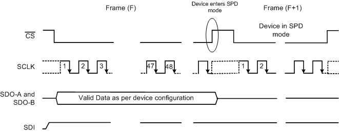 Figure 97. Enter SPD Mode
As shown in Figure 98, to exit SPD mode, the device must be selected (by bringing CS low) and SDI must be kept low for a minimum of 48 SCLK cycles during frame (F+3). The device starts powering-up on a CS rising edge following frame (F+3). After frame (F+3), a delay of tPU_SPD must elapse before programming the configuration register.
A valid write operation in frame (F+4) sets the device configuration for frame (F+5). Frame (F+4) must have at least 48 SCLK falling edges. The output data in frame (F+4) should be discarded.
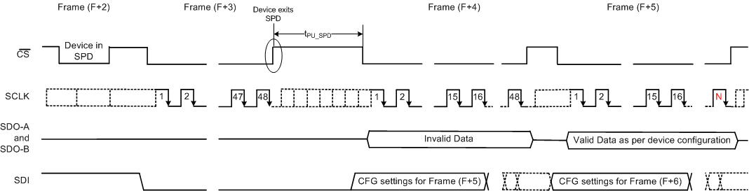
Refer to the Timing Characteristics: Serial Interface for timing specifications for this operating mode.
8.5.5 Frame Abort, Reconversion, or Short-Cycling
As discussed inFigure 99, the minimum number of SCLK falling edges (N) that must be provided between the beginning and end of the frame depends on the serial interface mode. The SCLK falling edges (N) program the device and retrieve the conversion result. If CS is brought high before the expected number of SCLK falling edges are provided, the current frame is aborted and the device starts sampling the new analog input signal.
If frame (F) is aborted, then the register write operation attempted in frame (F) is considered invalid and the internal registers are not updated. The device continues to have the same configuration in frame (F+1) from frame (F).
The output data bits latched before the CS rising edge are still valid data that correspond to sample N.
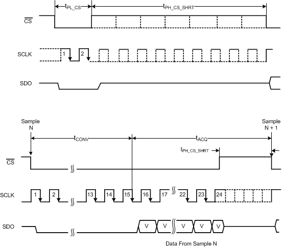 Figure 99. Frame Abort, Reconversion, or Short-Cycling Feature
Refer to the Timing Characteristics: Serial Interface for timing specifications for this operating mode.
9 Application and Implementation
9.1 Application Information
The two primary circuits required to maximize the performance of a high-precision, successive approximation register (SAR), analog-to-digital converter (ADC) are the input driver and the reference driver circuits. This section details some general principles for designing these circuits, and some application circuits designed using these devices.
The device supports operation either with an internal or external reference source. Refer to the Reference section for details about the decoupling requirements.
The reference source to the ADC must provide low-drift and very accurate dc voltage and support the dynamic charge requirements without affecting the noise and linearity performance of the device. The output broadband noise (typically in the order of a few 100 μVRMS) of the reference source must be appropriately filtered by using a low-pass filter with a cutoff frequency of a few hundred hertz. After band-limiting the noise from the reference source, the next important step is to design a reference buffer that can drive the dynamic load posed by the reference input of the ADC. At the start of each conversion, the reference buffer must regulate the voltage of the reference pin within 1 LSB of the intended value. This condition necessitates the use of a large filter capacitor at the reference pin of the ADC. The amplifier selected to drive the reference input pin must be stable while driving this large capacitor and should have low output impedance, low offset, and temperature drift specifications. To reduce the dynamic current requirements and crosstalk between the channels, a separate reference buffer is recommended for driving the reference input of each ADC channel.
The input driver circuit for a high-precision ADC mainly consists of two parts: a driving amplifier and a fly-wheel RC filter. The amplifier is used for signal conditioning of the input voltage and its low output impedance provides a buffer between the signal source and the switched capacitor inputs of the ADC. The RC filter helps attenuate the sampling charge injection from the switched-capacitor input stage of the ADC and functions as an antialiasing filter to band-limit the wideband noise contributed by the front-end circuit. Careful design of the front-end circuit is critical to meet the linearity and noise performance of a high-precision ADC.
9.1.1 Input Amplifier Selection
Selection criteria for the input amplifiers is highly dependent on the input signal type and the performance goals of the data acquisition system. Some key amplifier specifications to consider while selecting an appropriate amplifier to drive the inputs of the ADC are:
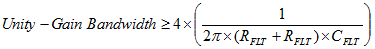
- Small-signal bandwidth. Select the small-signal bandwidth of the input amplifiers to be as high as possible after meeting the power budget of the system. Higher bandwidth reduces the closed-loop output impedance of the amplifier, thus allowing the amplifier to more easily drive the low cutoff frequency RC filter at the ADC inputs. Higher bandwidth also minimizes the harmonic distortion at higher input frequencies. In order to maintain the overall stability of the input driver circuit, the amplifier bandwidth should be selected as described in Equation 6:
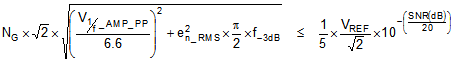
- Noise. Noise contribution of the front-end amplifiers should be as low as possible to prevent any degradation in SNR performance of the system. As a rule of thumb, to ensure that the noise performance of the data acquisition system is not limited by the front-end circuit, the total noise contribution from the front-end circuit should be kept below 20% of the input-referred noise of the ADC. Noise from the input driver circuit is band-limited by designing a low cutoff frequency RC filter and is calculated by Equation 7:
- V1 / f_AMP_PP is the peak-to-peak flicker noise in µV,
- en_RMS is the amplifier broadband noise density in nV/√Hz,
- f–3dB is the 3-dB bandwidth of the RC filter, and
- NG is the noise gain of the front-end circuit, which is equal to 1 in a buffer configuration.
- Distortion. Both the ADC and the input driver introduce nonlinearity in a data acquisition block. As a rule of thumb, to ensure that the distortion performance of the data acquisition system is not limited by the front-end circuit, the distortion of the input driver should be at least 10 dB lower than the distortion of the ADC, as shown in Equation 8.
- Settling Time. For dc signals with fast transients that are common in a multiplexed application, the input signal must settle to the desired accuracy at the inputs of the ADC during the acquisition time window. This condition is critical to maintain the overall linearity performance of the ADC. Typically, the amplifier data sheets specify the output settling performance only up to 0.1% to 0.001%, which may not be sufficient for the desired accuracy. Therefore, the settling behavior of the input driver should always be verified by TINA™-SPICE simulations before selecting the amplifier.
where

9.1.2 Antialiasing Filter
Converting analog-to-digital signals requires sampling an input signal at a constant rate. Any higher frequency content in the input signal beyond half the sampling frequency is digitized and folded back into the low-frequency spectrum. This process is called aliasing. Therefore, an analog, antialiasing filter must be used to remove the harmonic content from the input signal before being sampled by the ADC. An antialiasing filter is designed as a low-pass, RC filter, for which the 3-dB bandwidth is optimized based on specific application requirements. For dc signals with fast transients (including multiplexed input signals), a high-bandwidth filter is designed to allow accurately settling the signal at the ADC inputs during the small acquisition time window. For ac signals, the filter bandwidth should be kept low to band-limit the noise fed into the ADC input, thereby increasing the signal-to-noise ratio (SNR) of the system.
A filter capacitor, CFLT, connected across the ADC inputs (as shown in Figure 100), filters the noise from the front-end drive circuitry, reduces the sampling charge injection and provides a charge bucket to quickly charge the internal sample-and-hold capacitors during the acquisition process. As a rule of thumb, the value of this capacitor should be at least 10 times the specified value of the ADC sampling capacitance. For these devices, the input sampling capacitance is equal to 40 pF. Thus, the value of CFLT should be greater than 400 pF. The capacitor should be a COG- or NPO-type because these capacitor types have a high-Q, low-temperature coefficient, and stable electrical characteristics under varying voltages, frequency, and time.
Note that driving capacitive loads can degrade the phase margin of the input amplifiers, thus making the amplifier marginally unstable. To avoid amplifier stability issues, series isolation resistors (RFLT) are used at the output of the amplifiers. A higher value of RFLT is helpful from the amplifier stability perspective, but adds distortion as a result of interactions with the nonlinear input impedance of the ADC. Distortion increases with source impedance, input signal frequency, and input signal amplitude. Therefore, the selection of RFLT requires balancing the stability and distortion of the design. For these devices, TI recommends limiting the value of RFLT to a maximum of 22 Ω in order to avoid any significant degradation in linearity performance. The tolerance of the selected resistors can be chosen as 1% because the use of a differential capacitor at the input balances the effects resulting from any resistor mismatch.
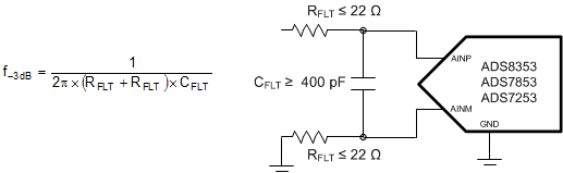 Figure 100. Antialiasing Filter
The input amplifier bandwidth should be much higher than the cutoff frequency of the antialiasing filter. TI strongly recommends performing a SPICE simulation to confirm that the amplifier has more than 40° phase margin with the selected filter. If an amplifier has less than a 40° phase margin with 22-Ω resistors, using a different amplifier with higher bandwidth or reducing the filter cutoff frequency with a larger differential capacitor is advisable.
9.2 Typical Applications
9.2.1 DAQ Circuit to Achieve Maximum SINAD for a 10-kHz Input Signal at Full Throughput
9.2.1.1 Design Requirements
To design an application circuit optimized to achieve target specifications listed in Table 20.
Table 20. Target Specifications
| TARGET SPECIFICATIONS | TEST CONDITIONS | ||||
|---|---|---|---|---|---|
| SNR | THD | DEVICE | INPUT SIGNAL FREQUENCY | THROUGHPUT | INTERFACE MODE |
| > 83 dB | < -100 dB | ADS8353 | 10 kHz | Maximum supported | 32-CLK, dual-SDO |
| > 81 dB | < –95 dB | ADS7853 | 10 kHz | Maximum supported | 32-CLK, dual-SDO |
| > 77.5 dB | < –85 dB | ADS7853 | 10 kHz | Maximum supported | 16-CLK, dual-SDO |
| > 71.5 dB | < –88 dB | ADS7253 | 10 kHz | Maximum supported | 32-CLK, dual-SDO |
| > 70.5 dB | < –80 dB | ADS7253 | 10 kHz | Maximum supported | 16-CLK, dual-SDO |
9.2.1.2 Detailed Design Procedure
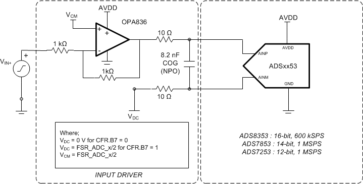
Best practice is for the distortion from the input driver to be at least 10 dB less than the ADC distortion. The distortion resulting from variation in the common-mode signal is eliminated by using the amplifier in an inverting gain configuration that establishes a fixed common-mode level for the circuit. This configuration also eliminates the requirement of rail-to-rail swing at the amplifier input. The low-power OPA836, used as an input driver, provides exceptional ac performance because of its extremely low-distortion and high-bandwidth specifications. In addition, the components of the antialiasing filter are such that the noise from the front-end circuit is kept low without adding distortion to the input signal.
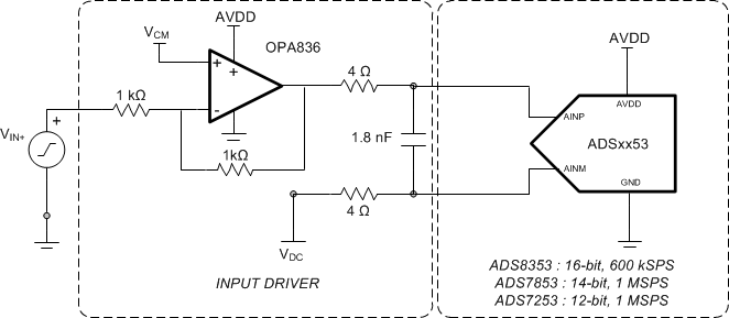
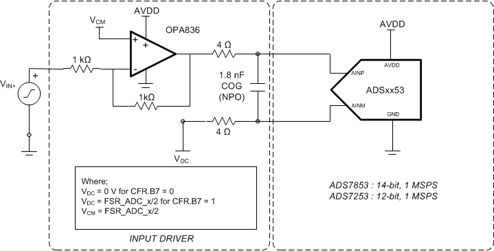
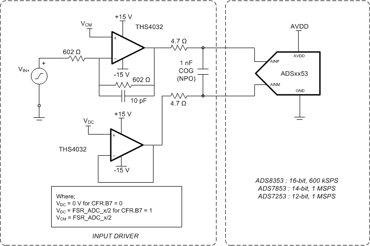
The application circuit illustrated in Figure 101 is optimized to achieve the lowest distortion and lowest noise for a
10-kHz input signal fed to the ADS8353 or ADS7853 or ADS7253 operating at full throughput with the default 32-CLK, dual-SDO interface mode. The input signal is processed through a high-bandwidth, low-distortion amplifier in an inverting gain configuration and a low-pass RC filter before being fed into the device.
The ADS7853 and the ADS7253 also support 16-CLK interface modes that achieve the rated throughput rate at much lower SCLK frequencies. However, when using the 16-CLK interface modes, the device receives less acquisition time when compared to the 32-CLK interface modes. The application circuit illustrated in Figure 102 is optimized to achieve the lowest distortion and lowest noise for a 10-kHz input signal fed to the ADS7853 or ADS7253 operating at full throughput with the 16-CLK, dual-SDO interface mode. The input signal is processed through a high-bandwidth, low-distortion amplifier in an inverting gain configuration and a low-pass RC filter before being fed into the device.
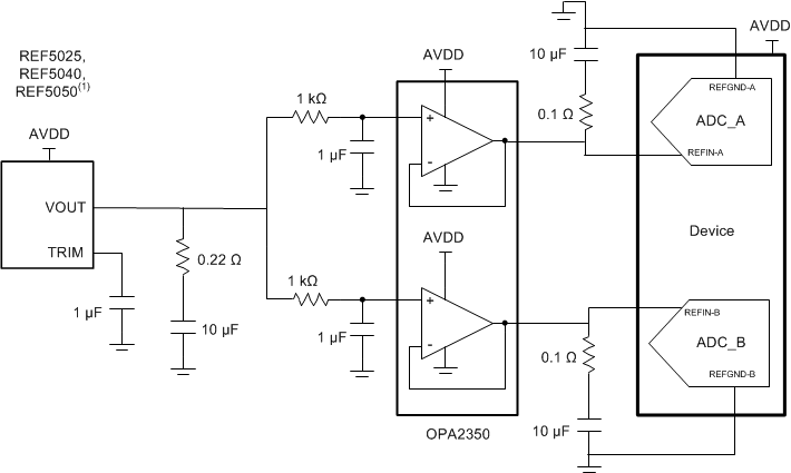
Figure 103 illustrates the reference driver circuit when operation with an external reference is desired. The reference voltage is generated by the high-precision, low-noise REF50xx circuit. The output broadband noise of the reference is heavily filtered by a low-pass filter with a 3-dB cutoff frequency of 160 Hz. The decoupling capacitor on each reference pin is selected to be 10 µF. The low output impedance, low noise, and fast settling time makes the OPA2350 a good choice for driving this high capacitive load.
9.2.1.3 Application Curves
To minimize external components and to maximize the dynamic range of the ADC, device is configured to operate with internal reference (CFR.B6 = 1) and 2 x VREF_x input full scale range (CFR.B9 = 1).
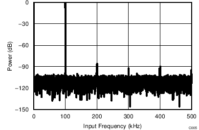
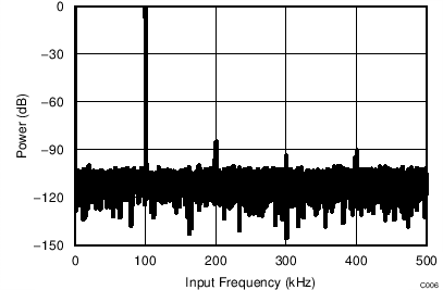
Figure 104, Figure 105, and Figure 106, show the FFT plots and test results obtained with the ADS8353, ADS7853, and ADS7253, respectively, operating at full throughput with a 32-CLK interface and the circuit configuration of Figure 101.
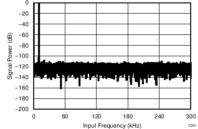
| SNR = 83.5 dB | THD = –101.2 dB | fIN = 10.1 kHz |
| SNR = 72.5 dB | THD = –94.2 dB | fIN = 10.1 kHz |
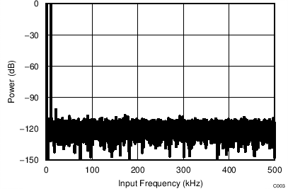
| SNR = 82.1 dB | THD = –98.2 dB | fIN = 10.1 kHz |
Figure 107 and Figure 108 show the FFT plots and test results obtained with the ADS7853 and ADS7253, respectively, operating at full throughput with 16-CLK interface and the circuit configuration of Figure 102.
| SNR = 78.1 dB | THD = –89.8 dB | fIN = 10.1 kHz |
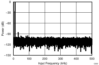
| SNR = 71.2 dB | THD = –84.9 dB | fIN = 10.1 kHz |
9.2.2 DAQ Circuit to Achieve Maximum SINAD for a 100-kHz Input Signal at Full Throughput
9.2.2.1 Design Requirements
To design an application circuit optimized to achieve target specifications listed in Table 21.
Table 21. Target Specifications
| TARGET SPECIFICATIONS | TEST CONDITIONS | ||||
|---|---|---|---|---|---|
| SNR | THD | DEVICE | INPUT SIGNAL FREQUENCY | THROUGHPUT | INTERFACE MODE |
| > 83 dB | < -95 dB | ADS8353 | 100 kHz | Maximum supported | 32-CLK, dual-SDO |
| > 78.5 dB | < –88 dB | ADS7853 | 100 kHz | Maximum supported | 32-CLK, dual-SDO |
| > 77.5 dB | < –85 dB | ADS7853 | 100 kHz | Maximum supported | 16-CLK, dual-SDO |
| > 71.5 dB | < –85 dB | ADS7253 | 100 kHz | Maximum supported | 32-CLK, dual-SDO |
| > 71 dB | < –84 dB | ADS7253 | 100 kHz | Maximum supported | 16-CLK, dual-SDO |
9.2.2.2 Detailed Design Procedure
Best practice is for the distortion from the input driver to be at least 10 dB less than the ADC distortion. The distortion resulting from variation in the common-mode signal is eliminated by using the amplifier in an inverting gain configuration that establishes a fixed common-mode level for the circuit. This configuration also eliminates the requirement of rail-to-rail swing at the amplifier input. The low-power OPA836, used as an input driver, provides exceptional ac performance because of its extremely low-distortion and high-bandwidth specifications. In addition, the components of the antialiasing filter are such that the noise from the front-end circuit is kept low without adding distortion to the input signal. To take full advantage of the pseudo-differential input structure of the ADC, the AINM pin must be driven to the appropriate VDC with the same amplifier and matching source impedance.
The application circuit illustrated in Figure 109 is optimized to achieve the lowest distortion and lowest noise for a 100-kHz input signal fed to the ADS8353 or ADS7853 or ADS7253 operating at full throughput. The THS4032, used as an input driver, provides exceptional ac performance because of its extremely low-distortion, low-noise, and high-bandwidth specifications. In addition, the components of the antialiasing filter are such that the noise from the front-end circuit is kept low without adding distortion to the input signal. External clamp circuit may be required to ensure that the inputs to the device do not exceed AVDD.
Figure 103 illustrates the reference driver circuit when operation with an external reference is desired. The reference voltage is generated by the high-precision, low-noise REF50xx circuit. The output broadband noise of the reference is heavily filtered by a low-pass filter with a 3-dB cutoff frequency of 160 Hz. The decoupling capacitor on each reference pin is selected to be 10 µF. The low output impedance, low noise, and fast settling time makes the OPA2350 a good choice for driving this high capacitive load.
9.2.2.3 Application Curves
To minimize external components and to maximize the dynamic range of the ADC, device is configured to operate with internal reference (CFR.B6 = 1) and 2 x VREF_x input full scale range (CFR.B9 = 1).
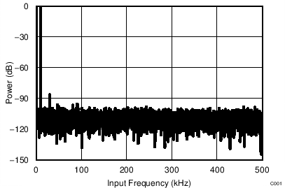
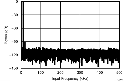
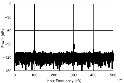
Figure 111, Figure 112, and Figure 113 show the FFT plots and test results obtained with the ADS8353, ADS7853 and ADS7253, respectively, operating at full throughput with a 32-CLK interface and the circuit configuration of Figure 109.
| SNR = 83.1 dB | THD = –95.5 dB | fIN = 100.2 kHz |
| SNR = 72.9 dB | THD = –85.8 dB | fIN = 100.2 kHz |
| SNR = 79.6 dB | THD = –90.9 dB | fIN = 100.2 kHz |
Figure 114 and Figure 115 show the FFT plots and test results obtained with the ADS7853 and ADS7253, respectively, operating with a 16-CLK interface and the circuit configuration of Figure 109.
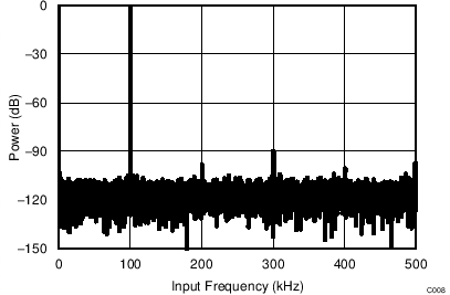
| SNR = 78.2 dB | THD = –87.2 dB | fIN = 100.2 kHz |
| SNR = 72.3 dB | THD = –84.3 dB | fIN = 100.2 kHz |
10 Power-Supply Recommendations
The devices have two separate power supplies: AVDD and DVDD. The device operates on AVDD; DVDD is used for the interface circuits. AVDD and DVDD can be independently set to any value within the permissible ranges.
When using the device with 2 × VREF input range (CFR.B9 = 1), the AVDD supply voltage value defines the permissible voltage swing on the analog input pins. To avoid saturation of output codes, and to use the full dynamic range on the analog input pins, AVDD must be set as shown in Equation 9, Equation 10, and Equation 11:
Decouple the AVDD and DVDD pins with the GND pin using individual 10-µF decoupling capacitors, as shown in Figure 116.
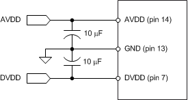 Figure 116. Power-Supply Decoupling
11 Layout
11.1 Layout Guidelines
Figure 117 shows a board layout example for the ADS8353, ADS7853, and ADS7253 with the WQFN package. Use a ground plane underneath the device and partition the PCB into analog and digital sections. Avoid crossing digital lines with the analog signal path and keep the analog input signals and the reference input signals away from noise sources. As shown in Figure 117, the analog input and reference signals are routed on the left side of the board and the digital connections are routed on the right side of the device.
The power sources to the device must be clean and well-bypassed. Use 10-μF, ceramic bypass capacitors in close proximity to the analog (AVDD) and digital (DVDD) power-supply pins. Avoid placing vias between the AVDD and DVDD pins and the bypass capacitors. Connect all ground pins to the ground plane using short, low impedance paths.
The REFIO-A and REFIO-B reference inputs and outputs are bypassed with 10-μF, X7R-grade, 0805-size, 16-V rated ceramic capacitors (CREF-x). Place the reference bypass capacitors as close as possible to the reference REFIO-x pins and connect the bypass capacitors using short, low-inductance connections. Avoid placing vias between the REFIO-x pins and the bypass capacitors. Small 0.1-Ω to 0.2-Ω resistors (RREF-x) are used in series with the reference bypass capacitors to improve stability.
The fly-wheel RC filters are placed immediately next to the input pins. Among ceramic surface-mount capacitors, COG (NPO) ceramic capacitors provide the best capacitance precision. The type of dielectric used in COG (NPO) ceramic capacitors provides the most stable electrical properties over voltage, frequency, and temperature changes. Figure 117 shows CIN-A and CIN-B filter capacitors placed across the analog input pins of the device.
11.2 Layout Example
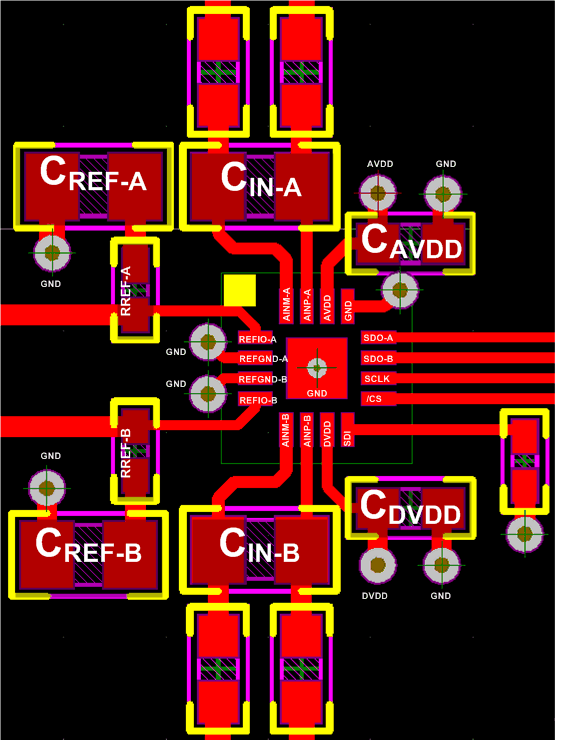 Figure 117. Recommended Layout
12 Device and Documentation Support
12.1 Related Links
The table below lists quick access links. Categories include technical documents, support and community resources, tools and software, and quick access to sample or buy.
Table 22. Related Links
| PARTS | PRODUCT FOLDER | SAMPLE & BUY | TECHNICAL DOCUMENTS | TOOLS & SOFTWARE | SUPPORT & COMMUNITY |
|---|---|---|---|---|---|
| ADS8353 | Click here | Click here | Click here | Click here | Click here |
| ADS7853 | Click here | Click here | Click here | Click here | Click here |
| ADS7253 | Click here | Click here | Click here | Click here | Click here |
12.2 Related Documentation
- TIPD117 Verified Design Reference Guide: 12 Bit 1 MSPS Single Supply Dual Channel Data Acquisition System for Optical Encoders in Motor Control Application Reference Design, SLAU517.
- REF5050 Data Sheet, SBOS410.
- OPA2350 Data Sheet, SBOS099.
- OPA836, OPA2836 Data Sheet, SLOS712.
- THS4032 Data Sheet, SLOS224.
12.3 Trademarks
TINA is a trademark of Texas Instruments Inc..
All other trademarks are the property of their respective owners.
12.4 Electrostatic Discharge Caution

This integrated circuit can be damaged by ESD. Texas Instruments recommends that all integrated circuits be handled with appropriate precautions. Failure to observe proper handling and installation procedures can cause damage.
ESD damage can range from subtle performance degradation to complete device failure. Precision integrated circuits may be more susceptible to damage because very small parametric changes could cause the device not to meet its published specifications.
12.5 Glossary
SLYZ022 — TI Glossary.
This glossary lists and explains terms, acronyms, and definitions.
13 Mechanical, Packaging, and Orderable Information
The following pages include mechanical packaging and orderable information. This information is the most current data available for the designated devices. This data is subject to change without notice and revision of this document. For browser-based versions of this data sheet, refer to the left-hand navigation.
IMPORTANT NOTICE
Texas Instruments Incorporated and its subsidiaries (TI) reserve the right to make corrections, enhancements, improvements and other changes to its semiconductor products and services per JESD46, latest issue, and to discontinue any product or service per JESD48, latest issue. Buyers should obtain the latest relevant information before placing orders and should verify that such information is current and complete. All semiconductor products (also referred to herein as "components") are sold subject to TI's terms and conditions of sale supplied at the time of order acknowledgment.
TI warrants performance of its components to the specifications applicable at the time of sale, in accordance with the warranty in TI's terms and conditions of sale of semiconductor products. Testing and other quality control techniques are used to the extent TI deems necessary to support this warranty. Except where mandated by applicable law, testing of all parameters of each component is not necessarily performed.
TI assumes no liability for applications assistance or the design of Buyers' products. Buyers are responsible for their products and applications using TI components. To minimize the risks associated with Buyers' products and applications, Buyers should provide adequate design and operating safeguards.
TI does not warrant or represent that any license, either express or implied, is granted under any patent right, copyright, mask work right, or other intellectual property right relating to any combination, machine, or process in which TI components or services are used. Information published by TI regarding third-party products or services does not constitute a license to use such products or services or a warranty or endorsement thereof. Use of such information may require a license from a third party under the patents or other intellectual property of the third party, or a license from TI under the patents or other intellectual property of TI.
Reproduction of significant portions of TI information in TI data books or data sheets is permissible only if reproduction is without alteration and is accompanied by all associated warranties, conditions, limitations, and notices. TI is not responsible or liable for such altered documentation. Information of third parties may be subject to additional restrictions.
Resale of TI components or services with statements different from or beyond the parameters stated by TI for that component or service voids all express and any implied warranties for the associated TI component or service and is an unfair and deceptive business practice. TI is not responsible or liable for any such statements.
Buyer acknowledges and agrees that it is solely responsible for compliance with all legal, regulatory and safety-related requirements concerning its products, and any use of TI components in its applications, notwithstanding any applications-related information or support that may be provided by TI. Buyer represents and agrees that it has all the necessary expertise to create and implement safeguards which anticipate dangerous consequences of failures, monitor failures and their consequences, lessen the likelihood of failures that might cause harm and take appropriate remedial actions. Buyer will fully indemnify TI and its representatives against any damages arising out of the use of any TI components in safety-critical applications.
In some cases, TI components may be promoted specifically to facilitate safety-related applications. With such components, TI's goal is to help enable customers to design and create their own end-product solutions that meet applicable functional safety standards and requirements. Nonetheless, such components are subject to these terms.
No TI components are authorized for use in FDA Class III (or similar life-critical medical equipment) unless authorized officers of the parties have executed a special agreement specifically governing such use.
Only those TI components which TI has specifically designated as military grade or "enhanced plastic" are designed and intended for use in military/aerospace applications or environments. Buyer acknowledges and agrees that any military or aerospace use of TI components which have not been so designated is solely at the Buyer's risk, and that Buyer is solely responsible for compliance with all legal and regulatory requirements in connection with such use.
TI has specifically designated certain components as meeting ISO/TS16949 requirements, mainly for automotive use. In any case of use of non-designated products, TI will not be responsible for any failure to meet ISO/TS16949.
Products
- Audio: www.ti.com/audio
- Amplifiers: amplifier.ti.com
- Data Converters: dataconverter.ti.com
- DLP® Products: www.dlp.com
- DSP: dsp.ti.com
- Clocks and Timers: www.ti.com/clocks
- Interface: interface.ti.com
- Logic: logic.ti.com
- Power Mgmt: power.ti.com
- Microcontrollers: microcontroller.ti.com
- RFID: www.ti.rfid.com
- OMAP Application Processors: www.ti.com/omap
- Wireless Connectivity: www.ti.com/wirelessconnectivity
Applications
- Automotive and Transportation: www.ti.com/automotive
- Communications and Telecom: www.ti.com/communications
- Computers and Peripherals: www.ti.com/computers
- Consumer Electronics: www.ti.com/consumer-apps
- Energy and Lighting: www.ti.com/energy
- Industrial: www.ti.com/industrial
- Medical: www.ti.com/medical
- Security: www.ti.com/security
- Space, Avionics and Defense: www.ti.com/space-avionics-defense
- Video & Imaging: www.ti.com/video
TI E2E Community : e2e.ti.com
Mailing Address: Texas Instruments, Post Office Box 655303, Dallas, Texas 75265
Copyright© 2014, Texas Instruments Incorporated