DATA SHEET
bq24311 Overvoltage and Overcurrent Protection IC and Li+ Charger Front-End Protection IC
1 Features
- Provides Protection for Three Variables:
- Input Overvoltage, with Rapid Response in < 1 μs
- User-Programmable Overcurrent with Current Limiting
- Battery Overvoltage
- 30 V Maximum Input Voltage
- Supports up to 0.3 A Input Current
- Robust Against False Triggering Due to Current Transients
- Thermal Shutdown
- Enable Input
- Status Indication – Fault Condition
2 Applications
- Mobile Phones and Smart Phones
- PDAs
- MP3 Players
- Low-Power Handheld Devices
- Bluetooth™ Headsets
3 Description
The bq24311 is a highly integrated circuit designed to protect Li-ion batteries from charging circuit failures. The IC continuously monitors the input voltage, input current, and battery voltage. The input overvoltage protection immediately removes power from the charging circuit by turning off an internal switch. The input protection limits the system current at the user-programmable value, and if the overcurrent persists, switches the pass element OFF after a blanking period. Additionally, the IC also monitors its own die temperature and switches off if it becomes too hot.
The IC can be controlled by a processor and also provides status information about fault conditions to the host.
Device Information
| PART NUMBER | PACKAGE | BODY SIZE (NOM) |
|---|---|---|
| bq24311 | WSON (8) | 2.00mm x 2.00mm |
- For all available packages, see the orderable addendum at the end of the datasheet.
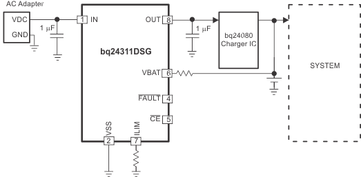
4 Application Information
5 Revision History
| Date | Revision | Notes |
|---|---|---|
| June | * | Initial release. |
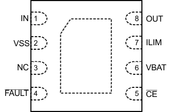
6 Pin Configuration and Functions
DSG PACKAGE
(TOP VIEW)
Pin Functions
| PIN | I/O | DESCRIPTION | ||
|---|---|---|---|---|
| NAME | DSG | |||
| IN | 1 | I | Input power, connect to external DC supply. Connect external 1μF ceramic capacitor (minimum) to VSS. | |
| OUT | 8 | O | Output pin to the charging system. Connect external 1 μF ceramic capacitor (minimum) to VSS. | |
| VBAT | 6 | I | Battery voltage sense input. Connect to pack positive pin through a resistor. | |
| ILIM | 7 | I/O | Input overcurrent threshold programming. Connect a resistor to VSS to set the overcurrent threshold. | |
| CE | 5 | I | Chip enable input. Active low. When CE = High, the input FET is off. Internally pulled down. | |
| FAULT | 4 | O | Device status, open-drain output. FAULT = Low indicates that the input FET Q1 has been turned on due to input overvoltage, input overcurrent, battery overvoltage, or thermal shutdown. | |
| VSS | 2 | – | Ground pin | |
| NC | 3 | This pin may have internal circuits used for test purposes. Do not make any external connections at these pins for normal operation. | ||
| Thermal PAD | – | There is an internal electrical connection between the exposed thermal pad and the VSS pin of the device. The thermal pad must be connected to the same potential as the VSS pin on the printed circuit board. Do not use the thermal pad as the primary ground input for the device. The VSS pin must be connected to ground at all times. | ||