-
bq78z100 Impedance Track Gas Gauge for 1-Series to 2-Series Li-Ion/Li-Polymer Battery Packs
- 1 Features
- 2 Applications
- 3 Description
- 4 Simplified Schematic
- 5 Revision History
- 6 Pin Configuration and Functions
-
7 Specifications
- 7.1 Absolute Maximum Ratings
- 7.2 ESD Ratings
- 7.3 Recommended Operating Conditions
- 7.4 Supply Current
- 7.5 Power Supply Control
- 7.6 Low-Voltage General Purpose I/O, TS1
- 7.7 Power-On Reset (POR)
- 7.8 Internal 1.8-V LDO
- 7.9 Current Wake Comparator
- 7.10 Coulomb Counter
- 7.11 ADC Digital Filter
- 7.12 ADC Multiplexer
- 7.13 Cell Balancing Support
- 7.14 Internal Temperature Sensor
- 7.15 NTC Thermistor Measurement Support
- 7.16 High-Frequency Oscillator
- 7.17 Low-Frequency Oscillator
- 7.18 Voltage Reference 1
- 7.19 Voltage Reference 2
- 7.20 Instruction Flash
- 7.21 Data Flash
- 7.22 Current Protection Thresholds
- 7.23 Current Protection Timing
- 7.24 N-CH FET Drive (CHG, DSG)
- 7.25 I2C and HDQ Interface I/O
- 7.26 I2C Interface Timing
- 7.27 HDQ Interface Timing
- 7.28 Typical Characteristics
-
8 Detailed Description
- 8.1 Overview
- 8.2 Functional Block Diagram
- 8.3
Feature Description
- 8.3.1 Battery Parameter Measurements
- 8.3.2 Coulomb Counter (CC)
- 8.3.3 CC Digital Filter
- 8.3.4 ADC Multiplexer
- 8.3.5 Analog-to-Digital Converter (ADC)
- 8.3.6 ADC Digital Filter
- 8.3.7 Internal Temperature Sensor
- 8.3.8 External Temperature Sensor Support
- 8.3.9 Power Supply Control
- 8.3.10 Power-On Reset
- 8.3.11 Bus Communication Interface
- 8.3.12 Cell Balancing Support
- 8.3.13 N-Channel Protection FET Drive
- 8.3.14 Low Frequency Oscillator
- 8.3.15 High Frequency Oscillator
- 8.3.16 1.8-V Low Dropout Regulator
- 8.3.17 Internal Voltage References
- 8.3.18 Overcurrent in Discharge Protection
- 8.3.19 Short-Circuit Current in Charge Protection
- 8.3.20 Short-Circuit Current in Discharge 1 and 2 Protection
- 8.3.21 Primary Protection Features
- 8.3.22 Gas Gauging
- 8.3.23 Charge Control Features
- 8.3.24 Authentication
- 8.4 Device Functional Modes
- 9 Applications and Implementation
- 10Power Supply Requirements
- 11Layout
- 12Device and Documentation Support
- 13Mechanical, Packaging, and Orderable Information
- IMPORTANT NOTICE
Package Options
Mechanical Data (Package|Pins)
- DRZ|12
Thermal pad, mechanical data (Package|Pins)
Orderable Information
bq78z100 Impedance Track Gas Gauge for 1-Series to 2-Series Li-Ion/Li-Polymer Battery Packs
1 Features
- High-Accuracy Coulomb Counter with Input Offset Error < 1 µV (Typical)
- High-Side FET Drive Allows Serial Bus Communication During Fault Conditions
- Analog Front End with Two Independent ADCs
- Support for Simultaneous Current and Voltage Sampling
- Bus Communications Interface Options
- I2C
- HDQ
- SHA-1 Hash Message Authentication Code (HMAC) Responder for Increased Battery Pack Security
- Split Key (2 × 64) Stored in Secure Memory
- Programmable Protection Levels for:
- Overcurrent in Discharge
- Short-Circuit Current in Charge
- Short-Circuit Current in Discharge
- Overvoltage
- Undervoltage
- Overtemperature
- Supports a 1-mΩ to 3-mΩ Current Sense Resistor
- Compact 12-Terminal SON Package (DRZ)
2 Applications
- Portable and Wearable Health Devices
- Portable Radios
- Industrial Data Collection
3 Description
The bq78z100 device provides a fully integrated pack-based solution with a flash programmable custom reduced instruction-set CPU (RISC), safety protection, and authentication for 1-series to 2-series cell Li-Ion and Li-Polymer battery packs.
The bq78z100 gas gauge communicates via an I2C-compatible interface or single-wire HDQ interface and combines an ultra-low-power, high-speed TI bqBMP processor, high-accuracy analog measurement capabilities, integrated flash memory, an array of peripheral and communication ports, an N-channel FET drive, and a SHA-1 Authentication transform responder into a complete, high-performance battery management solution.
The bq78z100 device provides an array of battery and system safety functions, including overcurrent in discharge, short circuit in charge, and short circuit in discharge protection for the battery, as well as FET protection for the N-channel FETs, internal AFE watchdog, and cell balancing. Through firmware, the devices can provide a larger array of features including protection against overvoltage, undervoltage, overtemperature, and more.
Device Information(1)
| PART NUMBER | PACKAGE | BODY SIZE (NOM) |
|---|---|---|
| bq78z100 | VSON (12) | 4.00 mm × 2.50 mm |
- For all available packages, see the orderable addendum at the end of the data sheet.
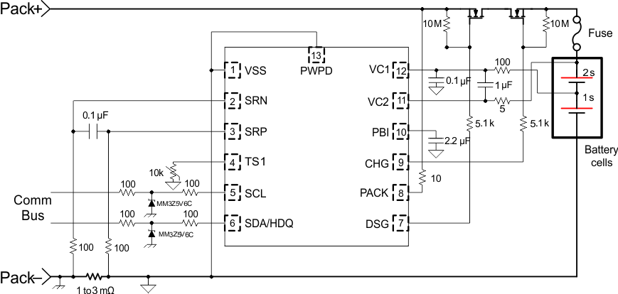
4 Simplified Schematic

5 Revision History
| DATE | REVISION | NOTES |
|---|---|---|
| September 2015 | * | Initial Release |
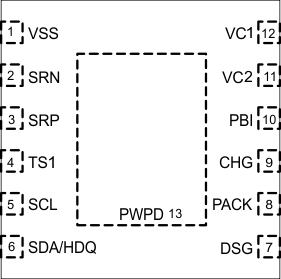
6 Pin Configuration and Functions

Pin Functions
| PIN | I/O | DESCRIPTION | |
|---|---|---|---|
| NAME | DRZ | ||
| VSS | 1 | P | Device ground |
| SRN | 2 | IA | Analog input pin connected to the internal coulomb counter peripheral for integrating a small voltage between SRP and SRN where SRP is the top of the sense resistor. |
| SRP | 3 | IA | Analog input pin connected to the internal coulomb counter peripheral for integrating a small voltage between SRP and SRN where SRP is the top of the sense resistor. |
| TS1 | 4 | IA | Input for ADC to the oversampled ADC channel |
| SCL | 5 | I/O | Serial Clock for the I2C interface; requires an external pullup when used |
| SDA/HDQ | 6 | I/O | Serial Data for the I2C and HDQ interfaces; requires an external pullup |
| DSG | 7 | O | N-Channel FET drive output pin |
| PACK | 8 | IA, P | Pack sense input pin |
| CHG | 9 | O | N-Channel FET drive output pin |
| PBI | 10 | P | Power supply backup input pin |
| VC2 | 11 | IA, P | Sense voltage input pin for most positive cell, balance current input for most positive cell. Primary power supply input and battery stack measurement input (BAT) |
| VC1 | 12 | IA | Sense voltage input pin for least positive cell, balance current input for least positive cell |
| PWPD | — | Exposed Pad, electrically connected to VSS (external trace) | |