-
CSD15380F3 20-V N-Channel FemtoFET MOSFET
Package Options
Mechanical Data (Package|Pins)
- YJM|3
Thermal pad, mechanical data (Package|Pins)
Orderable Information
CSD15380F3 20-V N-Channel FemtoFET MOSFET
1 Features
- Ultra-low CiSS and COSS
- Ultra-low Qg and Qgd
- Ultra-small footprint
- 0.73 mm × 0.64 mm
- Ultra-low profile
- 0.36-mm max height
- Integrated ESD protection diode
- Rated > 4-kV HBM
- Rated > 2-kV CDM
- Lead and halogen free
- RoHS compliant
2 Applications
- Optimized for load switch applications
- Optimized for general purpose switching applications
- Battery applications
- Handheld and mobile applications
3 Description
This 20-V, 990-mΩ, N-Channel FemtoFET™ MOSFET is designed and optimized to minimize the footprint in many handheld and mobile applications. Ultra-low capacitance improves switching speeds. When used in data line applications, the low capacitance minimizes noise coupling. This technology is capable of replacing standard small signal MOSFETs while providing a substantial reduction in footprint size.
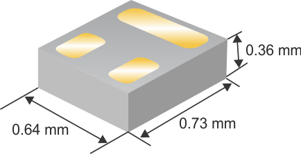 Typical Part Dimensions
| TA = 25°C | TYPICAL VALUE | UNIT | ||
|---|---|---|---|---|
| VDS | Drain-to-Source Voltage | 20 | V | |
| Qg | Gate Charge Total (4.5 V) | 0.216 | nC | |
| Qgd | Gate Charge Gate-to-Drain | 0.027 | nC | |
| RDS(on) | Drain-to-Source On-Resistance |
VGS = 2.5 V | 2220 | mΩ |
| VGS = 4.5 V | 1170 | |||
| VGS = 8 V | 990 | |||
| VGS(th) | Threshold Voltage | 1.1 | V | |
| DEVICE | QTY | MEDIA | PACKAGE | SHIP |
|---|---|---|---|---|
| CSD15380F3 | 3000 | 7-Inch Reel | Femto 0.73-mm × 0.64-mm Land Grid Array (LGA) |
Tape and Reel |
| CSD15380F3T | 250 |
| TA = 25°C (unless otherwise stated) | VALUE | UNIT | |
|---|---|---|---|
| VDS | Drain-to-Source Voltage | 20 | V |
| VGS | Gate-to-Source Voltage | 10 | V |
| ID | Continuous Drain Current(1) | 0.9 | A |
| Continuous Drain Current(2) | 0.5 | ||
| IDM | Pulsed Drain Current(3) | 1.6 | A |
| PD | Power Dissipation(1) | 1.4 | W |
| Power Dissipation(2) | 0.5 | ||
| V(ESD) | Human-Body Model (HBM) | 4 | kV |
| Charged-Device Model (CDM) | 2 | ||
| TJ, Tstg |
Operating Junction and Storage Temperature |
–55 to 150 | °C |
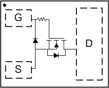 Top View
4 Revision History
Changes from Revision A (July 2017) to Revision B (February 2022)
- Changed ultra-low profile bullet from 0.35 mm to 0.36 mm in height.Go
- Updated ultra-low profile image height from 0.35 mm to 0.36 mm.Go
- Changed ultra-low profile image height from 0.35 mm to 0.36 mm.Go
- Added FemtoFET Surface Mount Guide note.Go
Changes from Revision A (July 2017) to Revision B (November 2018)
5 Specifications
5.1 Electrical Characteristics
| PARAMETER | TEST CONDITIONS | MIN | TYP | MAX | UNIT | ||
|---|---|---|---|---|---|---|---|
| STATIC CHARACTERISTICS | |||||||
| BVDSS | Drain-to-source voltage | VGS = 0 V, IDS = 250 μA | 20 | V | |||
| IDSS | Drain-to-Source leakage current | VGS = 0 V, VDS = 16 V | 50 | nA | |||
| IGSS | Gate-to-source leakage current | VDS = 0 V, VGS = 10 V | 25 | nA | |||
| VGS(th) | Gate-to-source threshold voltage | VDS = VGS, IDS = 2.5 μA | 0.85 | 1.10 | 1.35 | V | |
| RDS(on) | Drain-to-source on-resistance | VGS = 2.5 V, IDS = 0.1 A | 2220 | 4000 | mΩ | ||
| VGS = 4.5 V, IDS = 0.1 A | 1170 | 1460 | |||||
| VGS = 8 V, IDS = 0.1 A | 990 | 1190 | |||||
| gfs | Transconductance | VDS = 2 V, IDS = 0.1 A | 0.64 | S | |||
| DYNAMIC CHARACTERISTICS | |||||||
| Ciss | Input capacitance | VGS = 0 V, VDS = 10 V, ƒ = 1 MHz |
8.1 | 10.5 | pF | ||
| Coss | Output capacitance | 5.9 | 7.7 | pF | |||
| Crss | Reverse transfer capacitance | 0.13 | 0.17 | pF | |||
| RG | Series gate resistance | 9.6 | Ω | ||||
| Qg | Gate charge total (4.5 V) | VDS = 10 V, IDS = 0.1 A | 0.216 | 0.281 | nC | ||
| Qgd | Gate charge gate-to-drain | 0.027 | nC | ||||
| Qgs | Gate charge gate-to-source | 0.077 | nC | ||||
| Qg(th) | Gate charge at Vth | 0.048 | nC | ||||
| td(on) | Turnon delay time | VDS = 10 V, VGS = 4.5 V, IDS = 0.1 A, RG = 0 Ω |
3 | ns | |||
| tr | Rise time | 1 | ns | ||||
| td(off) | Turnoff delay time | 7 | ns | ||||
| tf | Fall time | 7 | ns | ||||
| DIODE CHARACTERISTICS | |||||||
| VSD | Diode forward voltage | ISD = 0.1 A, VGS = 0 V | 0.85 | 1 | V | ||
5.2 Thermal Information
| THERMAL METRIC | TYPICAL VALUES | UNIT | |||
|---|---|---|---|---|---|
| RθJA | Junction-to-ambient thermal resistance(1) | 90 | °C/W | ||
| Junction-to-ambient thermal resistance(2) | 255 | ||||
5.3 Typical MOSFET Characteristics
TA = 25°C (unless otherwise stated)
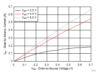 Figure 5-1 Saturation Characteristics
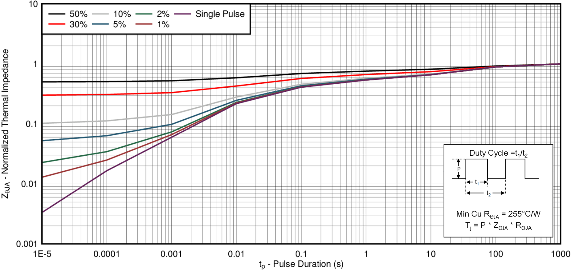 Figure 5-3 Transient Thermal Impedance
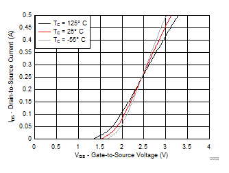
| VDS = 5 V | ||
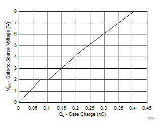
| VDS = 10 V | ID = 0.1 A | ||
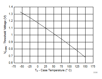
| ID = 2.5 µA | ||
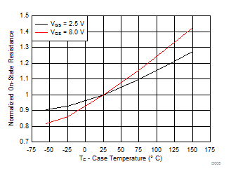
| ID = 0.1 A | ||
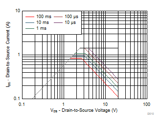
| Single pulse, typical RθJA = 255°C/W (min Cu) | ||
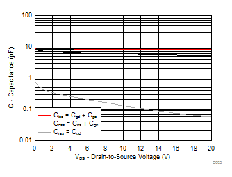 Figure 5-5 Capacitance
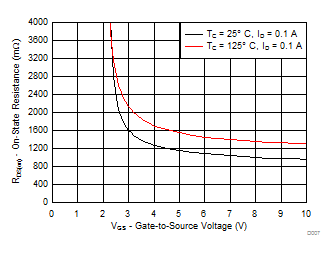 Figure 5-7 On-State Resistance vs Gate-to-Source Voltage
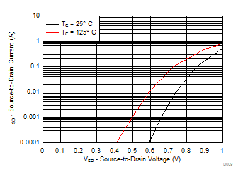 Figure 5-9 Typical Diode Forward Voltage
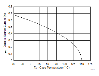 Figure 5-11 Maximum Drain Current vs Temperature
6 Device and Documentation Support
6.1 Receiving Notification of Documentation Updates
To receive notification of documentation updates, navigate to the device product folder on ti.com. In the upper right corner, click on Alert me to register and receive a weekly digest of any product information that has changed. For change details, review the revision history included in any revised document.
6.2 Trademarks
FemtoFET are trademarks of Texas Instruments.
All trademarks are the property of their respective owners.