-
CSD18531Q5A 60-V N-Channel NexFET™ Power MOSFET
Package Options
Refer to the PDF data sheet for device specific package drawings
Mechanical Data (Package|Pins)
- DQJ|8
Thermal pad, mechanical data (Package|Pins)
Orderable Information
DATA SHEET
CSD18531Q5A 60-V N-Channel NexFET™ Power MOSFET
1 Features
2 Applications
- DC-DC Conversion
- Secondary Side Synchronous Rectifier
- Battery Motor Control
3 Description
This 60-V, 3.5-mΩ, 5-mm × 6-mm NexFET™ power MOSFET is designed to minimize losses in power conversion applications.
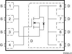
Top View
Product Summary
Device Information(1)
| DEVICE | QTY | MEDIA | PACKAGE | SHIP |
|---|---|---|---|---|
| CSD18531Q5A | 2500 | 13-Inch Reel | SON 5.00-mm × 6.00-mm Plastic Package |
Tape and Reel |
| CSD18531Q5AT | 250 | 7-Inch Reel |
- For all available packages, see the orderable addendum at the end of the data sheet.
Absolute Maximum Ratings
| TA = 25°C | VALUE | UNIT | |
|---|---|---|---|
| VDS | Drain-to-Source Voltage | 60 | V |
| VGS | Gate-to-Source Voltage | ±20 | V |
| ID | Continuous Drain Current (Package Limited) | 100 | A |
| Continuous Drain Current (Silicon Limited), TC = 25°C | 134 | ||
| Continuous Drain Current(1) | 19 | ||
| IDM | Pulsed Drain Current(2) | 400 | A |
| PD | Power Dissipation(1) | 3.8 | W |
| Power Dissipation, TC = 25°C | 156 | ||
| TJ | Operating Junction | –55 to 175 | °C |
| Tstg | Storage Temperature | –55 to 175 | °C |
| EAS | Avalanche Energy, Single Pulse ID = 67 A, L = 0.1 mH, RG = 25 Ω |
224 | mJ |
4 Revision History
Changes from F Revision (October 2016) to G Revision
- Changed temperature range from 150°C : to 175°CGo
- Changed IDM using 175°C data from 370 A : to 400 AGo
- Changed PD using 175°C data from 3.1 W : to 3.8 WGo
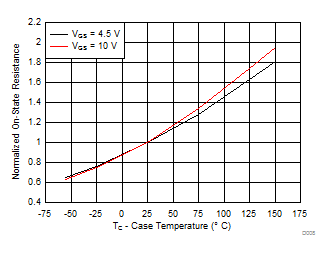
- Changed Figure 6 to extend to 175°CGo
- Changed Figure 8 to extend to 175°CGo
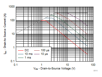
- Changed Figure 10 using 175°C dataGo
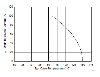
- Changed Figure 12 to extend to 175°CGo
Changes from E Revision (August 2015) to F Revision
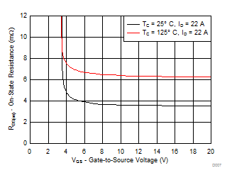
- Changed the 125°C RDS(on) vs VGS curve to reflect typical part characterizationGo
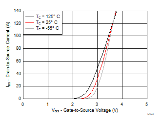
- Changed the 125°C curve in Figure 7 to reflect typical part characterizationGo
- Added Receiving Notification of Documentation Updates section to the Device and Documentation Support sectionGo
Changes from D Revision (May 2015) to E Revision
Changes from C Revision (March 2015) to D Revision
- Added Community Resources. Go
Changes from B Revision (October 2012) to C Revision
- Added part number to title. Go
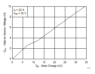
- Changed Qg value to 36 nC, measured at 10 V. Go
- Added 7" reel to Ordering Information. Go
- Increase max pulsed current to 370 A. Go
- Added line for max power dissipation with the case temperature held to 25°C.Go
- Updated pulsed current conditions. Go
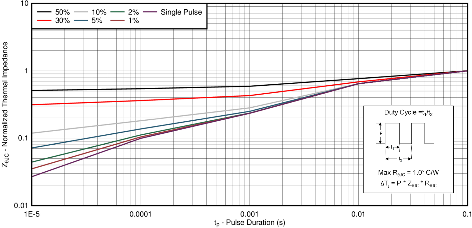
- Updated Figure 1 to show ZθJC curves.Go
- Updated Figure 10Go
- Updated Figure 12. Go
Changes from A Revision (June 2012) to B Revision
- Changed the Transconductance TYP value From: 177 S To: 128 S.Go
- Changed the Turn On and Turn Off Delay Time, Rise and Fall Time Test. Conditions From: IDS = 22 A, RG = 2 Ω To: IDS = 22 A, RG = 0 Ω. Go
- Changed the Qrr Reverse Recovery Charge TYP value From: 68 nC To: 100 nC. Go
Changes from * Revision (June 2012) to A Revision
- Added TA = 25°C to the Product Summary tableGo
5 Specifications
5.1 Electrical Characteristics
TA = 25°C (unless otherwise stated)5.2 Thermal Information
TA = 25°C (unless otherwise stated)| THERMAL METRIC | MIN | TYP | MAX | UNIT | |
|---|---|---|---|---|---|
| RθJC | Junction-to-case thermal resistance(1) | 1.0 | °C/W | ||
| RθJA | Junction-to-ambient thermal resistance(1)(2) | 50 | °C/W | ||
(1) RθJC is determined with the device mounted on a 1-in2 (6.45-cm2), 2-oz (0.071-mm) thick Cu pad on a 1.5-in × 1.5-in (3.81-cm × 3.81-cm), 0.06-in (1.52-mm) thick FR4 PCB. RθJC is specified by design, whereas RθJA is determined by the user’s board design.
(2) Device mounted on FR4 material with 1-in2 (6.45-cm2), 2-oz (0.071-mm) thick Cu.
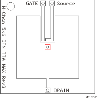 |
Max RθJA = 50°C/W when mounted on 1 in2 (6.45 cm2) of 2-oz (0.071-mm) thick Cu. |
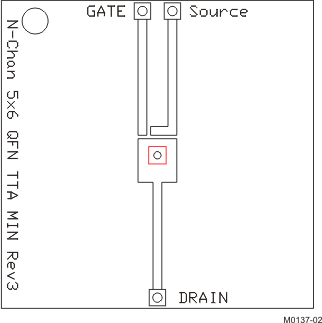 |
Max RθJA = 125°C/W when mounted on a minimum pad area of 2-oz (0.071-mm) thick Cu. |
5.3 Typical MOSFET Characteristics
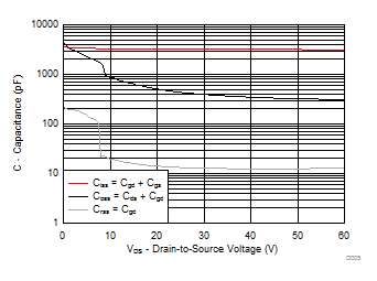
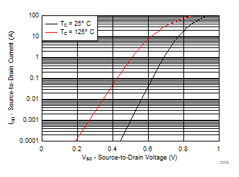
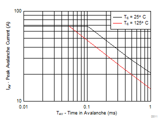
TA = 25°C (unless otherwise stated)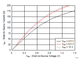
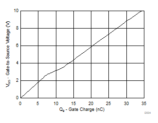
| VDS = 30 V | ID = 22 A |
