-
CSD87502Q2 30 V Dual N-Channel NexFET™ Power MOSFETs
Package Options
Refer to the PDF data sheet for device specific package drawings
Mechanical Data (Package|Pins)
- DLV|6
Thermal pad, mechanical data (Package|Pins)
Orderable Information
DATA SHEET
CSD87502Q2 30 V Dual N-Channel NexFET™ Power MOSFETs
1 Features
- Low On-Resistance
- Dual Independent MOSFETs
- Space Saving SON 2 × 2 mm Plastic Package
- Optimized for 5 V Gate Driver
- Avalanche Rated
- Pb and Halogen Free
- RoHS Compliant
2 Applications
- Point-of-Load Synchronous Buck Converter for Applications in Networking, Telecom, and Computing Systems
- Adaptor or USB Input Protection for Notebook PCs and Tablets
- Battery Protection
3 Description
The CSD87502Q2 is a 30 V, 27 mΩ N-Channel device with dual independent MOSFETs in a SON 2 x 2 mm plastic package. The two FETs were designed to be used in a half-bridge configuration for synchronous buck and other power supply applications. Additionally, these NexFET™ power MOSFETs can be used for adaptor, USB input protection, and battery charging applications. The dual FETs feature low drain-to-source on-resistance that minimizes losses and offers low component count for space-constrained applications.
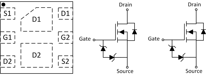
Top View and Circuit Image
Product Summary
| TA = 25°C | TYPICAL VALUE | UNIT | ||
|---|---|---|---|---|
| VDS | Drain-to-Source Voltage | 30 | V | |
| Qg | Gate Charge Total (4.5 V) | 2.2 | nC | |
| Qgd | Gate Charge Gate to Drain | 0.5 | nC | |
| RDS(on) | Drain-to-Source On Resistance | VGS = 3.8 V | 42.0 | mΩ |
| VGS = 4.5 V | 35.5 | mΩ | ||
| VGS = 10 V | 27.0 | mΩ | ||
| VGS(th) | Threshold Voltage | 1.6 | V | |
.
Ordering Information(1)
| DEVICE | MEDIA | QTY | PACKAGE | SHIP |
|---|---|---|---|---|
| CSD87502Q2 | 7-Inch Reel | 3000 | SON 2 x 2 mm Plastic Package |
Tape and Reel |
| CSD87502Q2T | 7-Inch Reel | 250 |
- For all available packages, see the orderable addendum at the end of the data sheet.
Absolute Maximum Ratings
| TA = 25°C | VALUE | UNIT | |
|---|---|---|---|
| VDS | Drain-to-Source Voltage | 30 | V |
| VGS | Gate-to-Source Voltage | ±20 | V |
| ID | Continuous Drain Current (Package limited) | 5.0 | A |
| IDM | Pulsed Drain Current(1) | 23 | A |
| PD | Power Dissipation(2) | 2.3 | W |
| TJ, Tstg |
Operating Junction Temperature, Storage Temperature |
–55 to 150 | °C |
| EAS | Avalanche Energy, single pulse ID = 7.9 A, L = 0.1 mH, RG = 25 Ω |
3.1 | mJ |
- Max RθJA = 185 °C/W, pulse duration ≤100 μs, duty cycle ≤1%.
- Typical RθJA = 55 °C/W on a 1 inch2, 2 oz. Cu pad on a 0.06 inch thick FR4 PCB.
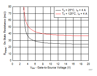
RDS(on) vs VGS |
Gate Charge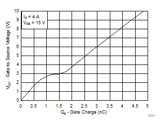 |
4 Revision History
| DATE | REVISION | NOTES |
|---|---|---|
| December 2015 | * | Initial release. |
5 Specifications
5.1 Electrical Characteristics
(TA = 25°C unless otherwise stated)| PARAMETER | TEST CONDITIONS | MIN | TYP | MAX | UNIT | ||
|---|---|---|---|---|---|---|---|
| STATIC CHARACTERISTICS | |||||||
| BVDSS | Drain-to-source voltage | VGS = 0 V, ID = 250 μA | 30 | V | |||
| IDSS | Drain-to-source leakage current | VGS = 0 V, VDS = 24 V | 1 | μA | |||
| IGSS | Gate-to-source leakage current | VDS = 0 V, VGS = 20 V | 4 | μA | |||
| VGS(th) | Gate-to-source threshold voltage | VDS = VGS, ID = 250 μA | 1.2 | 1.6 | 2.0 | V | |
| RDS(on) | Drain-to-source on-resistance | VGS = 3.8 V, ID = 4 A | 42.0 | 60.0 | mΩ | ||
| VGS = 4.5 V, ID = 4 A | 35.5 | 42.0 | mΩ | ||||
| VGS = 10 V, ID = 4 A | 27.0 | 32.4 | mΩ | ||||
| gfs | Transconductance | VDS = 3 V, ID = 4 A | 75 | S | |||
| DYNAMIC CHARACTERISTICS | |||||||
| Ciss | Input capacitance | VGS = 0 V, VDS = 15 V, ƒ = 1 MHz | 272 | 353 | pF | ||
| Coss | Output capacitance | 42 | 55 | pF | |||
| Crss | Reverse transfer capacitance | 22 | 29 | pF | |||
| RG | Series gate resistance | 6.9 | Ω | ||||
| Qg | Gate charge total (4.5 V) | VDS = 15 V, ID = 4 A | 2.2 | 2.9 | nC | ||
| Qg | Gate charge total (10 V) | 4.6 | 6.0 | nC | |||
| Qgd | Gate charge gate to drain | 0.5 | nC | ||||
| Qgs | Gate charge gate to source | 1.0 | nC | ||||
| Qg(th) | Gate charge at Vth | 0.5 | nC | ||||
| Qoss | Output charge | VDS = 15 V, VGS = 0 V | 1.4 | nC | |||
| td(on) | Turn on delay time | VDS = 15 V, VGS = 5 V, IDS = 4 A, RG = 0 Ω |
3 | ns | |||
| tr | Rise time | 11 | ns | ||||
| td(off) | Turn off delay time | 12 | ns | ||||
| tf | Fall time | 3 | ns | ||||
| DIODE CHARACTERISTICS | |||||||
| VSD | Diode forward voltage | ISD = 4 A, VGS = 0 V | 0.85 | 1.0 | V | ||
| Qrr | Reverse recovery charge | VDS= 15 V, IF = 4 A, di/dt = 300 A/μs |
4.0 | nC | |||
| trr | Reverse recovery time | 6.4 | ns | ||||
5.2 Thermal Information
(TA = 25°C unless otherwise stated)| THERMAL METRIC | MIN | TYP | MAX | UNIT | |
|---|---|---|---|---|---|
| RθJA | Junction-to-ambient thermal resistance(1) | 70 | °C/W | ||
| Junction-to-ambient thermal resistance(2) | 185 | ||||
(1) Device mounted on FR4 material with 1 inch2 (6.45 cm2), 2 oz. (0.071 mm thick) Cu.
(2) Device mounted on FR4 material with minimum Cu mounting area.
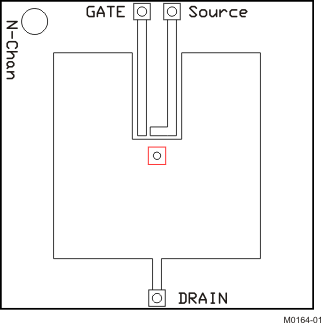 |
Max RθJA = 70 when mounted on 1 inch2 (6.45 cm2) of 2 oz. (0.071 mm thick) Cu. |
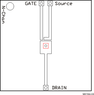 |
Max RθJA = 185 when mounted on minimum pad area of 2 oz. (0.071 mm thick) Cu. |
5.3 Typical MOSFET Characteristics
(TA = 25°C unless otherwise stated)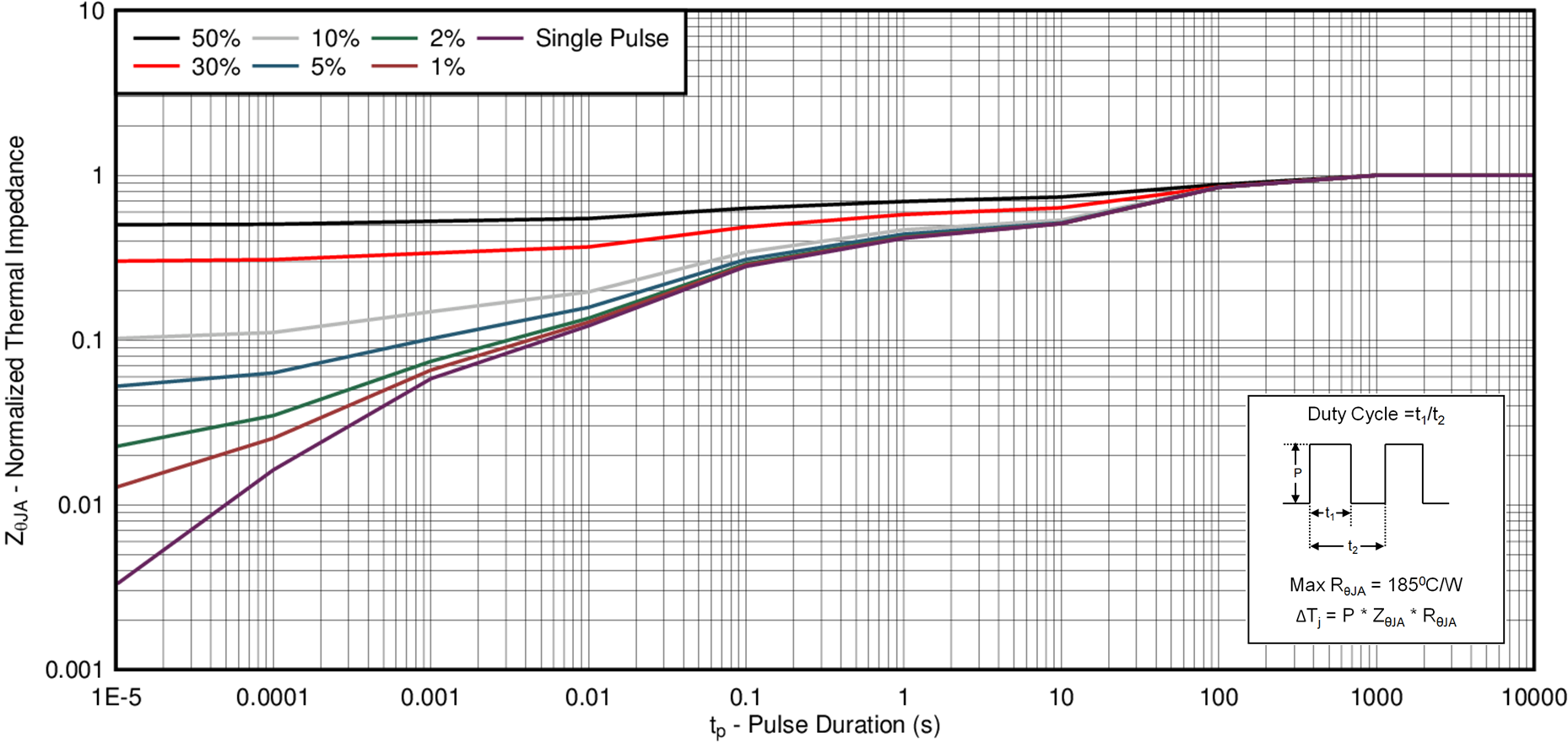
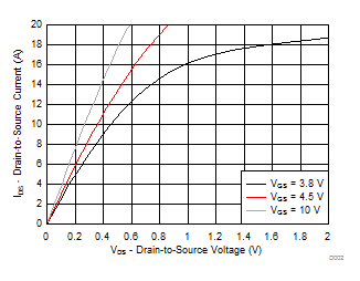
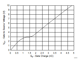
| ID = 4 A | VDS = 15 V | |
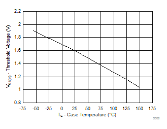
| ID = 4 A | ||
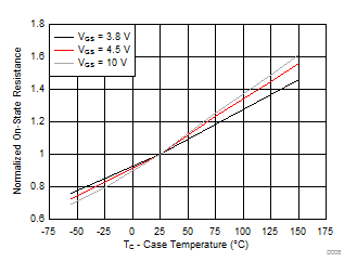
| ID = 4 A | ||
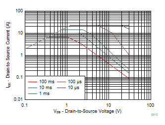
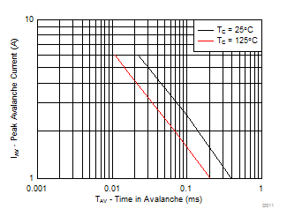
| Single Pulse, Max RθJA = 185°C/W | ||
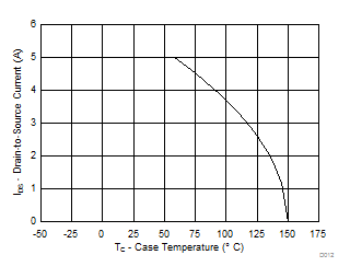
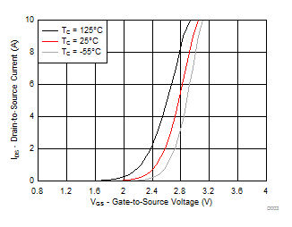
| VDS = 5 V | ||

