-
DAC082S085 8-Bit Micro Power DUAL Digital-to-Analog Converter With Rail-to-Rail Output
- 1 Features
- 2 Applications
- 3 Description
- 4 Revision History
- 5 Description (continued)
- 6 Pin Configuration and Functions
- 7 Specifications
- 8 Detailed Description
- 9 Application and Implementation
- 10Power Supply Recommendations
- 11Layout
- 12Device and Documentation Support
- 13Mechanical, Packaging, and Orderable Information
- IMPORTANT NOTICE
Package Options
Mechanical Data (Package|Pins)
Thermal pad, mechanical data (Package|Pins)
- DSC|10
Orderable Information
DAC082S085 8-Bit Micro Power DUAL Digital-to-Analog Converter With Rail-to-Rail Output
1 Features
- Ensured Monotonicity
- Low Power Operation
- Rail-to-Rail Voltage Output
- Power-On Reset to 0 V
- Simultaneous Output Updating
- Wide Power Supply Range: 2.7 V to 5.5 V
- Industry's Smallest Package
- Power-Down Modes
- Key Specifications:
- Resolution: 8 Bits
- INL: ±0.5 LSB (Maximum)
- DNL: 0.18 / –0.13 LSB (Maximum)
- Settling Time: 4.5 µs (Maximum)
- Zero Code Error: 15 mV (Maximum)
- Full-Scale Error: –0.75% FS (Maximum)
- Supply Power:
- Normal: 0.6 mW (3 V) / 1.6 mW (5 V) (Typical)
- Power Down: 0.3 µW (3 V) / 0.8 µW (5 V) (Typical)
2 Applications
3 Description
The DAC082S085 device is a full-featured, general-purpose, DUAL, 8-bit, voltage-output, digital-to-analog converter (DAC) that can operate from a single 2.7-V to 5.5-V supply and consumes 0.6 mW at 3 V and 1.6 mW at 5 V. The DAC082S085 is packaged in 10-pin SON and VSSOP packages. The 10-pin WSON package makes the DAC082S085 the smallest DUAL DAC in its class. The on-chip output amplifier allows rail-to-rail output swing, and the three-wire serial interface operates at clock rates up to 40 MHz over the entire supply voltage range. Competitive devices are limited to 25-MHz clock rates at supply voltages in the 2.7 V to 3.6 V range. The serial interface is compatible with standard SPI™, QSPI, MICROWIRE, and DSP interfaces.
Device Information(1)
| PART NUMBER | PACKAGE | BODY SIZE (NOM) |
|---|---|---|
| DAC082S085 | VSSOP (10) | 3.00 mm × 3.00 mm |
| WSON (10) | 3.00 mm × 3.00 mm |
- For all available packages, see the orderable addendum at the end of the data sheet.
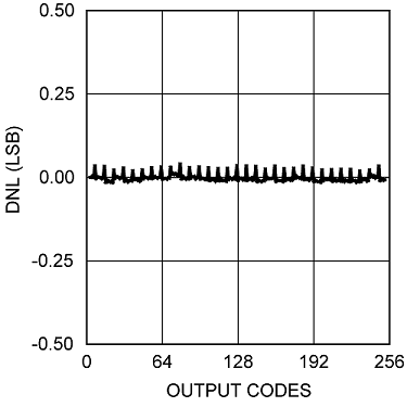
DNL at VA = 3 V
4 Revision History
Changes from F Revision (March 2013) to G Revision
- Added ESD Ratings table, Feature Description section, Device Functional Modes, Application and Implementation section, Power Supply Recommendations section, Layout section, Device and Documentation Support section, and Mechanical, Packaging, and Orderable Information section Go
- Changed Thermal Information table Go
Changes from E Revision (March 2013) to F Revision
- Changed layout of National Data Sheet to TI formatGo
5 Description (continued)
The reference for the DAC082S085 serves both channels and can vary in voltage between 1 V and VA, providing the widest possible output dynamic range. The DAC082S085 has a 16-bit input shift register that controls the outputs to be updated, the mode of operation, the power-down condition, and the binary input data. Both outputs can be updated simultaneously or individually depending on the setting of the two mode of operation bits.
A power-on reset circuit ensures that the DAC output powers up to 0 V and remains there until there is a valid write to the device. A power-down feature reduces power consumption to less than a microWatt with three different termination options.
The low power consumption and small packages of the DAC082S085 make it an excellent choice for use in battery-operated equipment.
The DAC082S085 is one of a family of pin-compatible DACs, including the 10-bit DAC102S085 and the 12-bit DAC124S085. The DAC082S085 operates over the extended industrial temperature range of −40°C to 105°C.
6 Pin Configuration and Functions
Pin Functions
| PIN | TYPE | DESCRIPTION | |
|---|---|---|---|
| NO. | NAME | ||
| 1 | VA | Supply | Power supply input. Must be decoupled to GND. |
| 2 | VOUTA | Analog Output | Channel A analog output voltage. |
| 3 | VOUTB | Analog Output | Channel B analog output voltage. |
| 4 | NC | — | Not connected |
| 5 | NC | — | Not connected |
| 6 | GND | Ground | Ground reference for all on-chip circuitry. |
| 7 | VREFIN | Analog Input | Unbuffered reference voltage shared by all channels. Must be decoupled to GND. |
| 8 | DIN | Digital Input | Serial data input. Data is clocked into the 16-bit shift register on the falling edges of SCLK after the fall of SYNC. |
| 9 | SYNC | Digital Input | Frame synchronization input for the data input. When this pin goes low, it enables the input shift register and data is transferred on the falling edges of SCLK. The DAC is updated on the 16th clock cycle unless SYNC is brought high before the 16th clock, in which case the rising edge of SYNC acts as an interrupt and the write sequence is ignored by the DAC. |
| 10 | SCLK | Digital Input | Serial clock input. Data is clocked into the input shift register on the falling edges of this pin. |
| PAD | PAD | Ground | Exposed die attach pad can be connected to ground or left floating. Soldering the pad to the PCB offers optimal thermal performance and enhances package self-alignment during reflow. |
7 Specifications
7.1 Absolute Maximum Ratings
over operating free-air temperature range (unless otherwise noted)(1)(2)(3)| MIN | MAX | UNIT | ||
|---|---|---|---|---|
| Supply voltage, VA | 6.5 | V | ||
| Voltage on any input pin | –0.3 | 6.5 | V | |
| Input current at any pin(4) | 10 | mA | ||
| Package input current(4) | 20 | mA | ||
| Power consumption at TA = 25°C | See(5) | |||
| Junction temperature, TJ | 150 | °C | ||
| Storage temperature, Tstg | –65 | 150 | °C | |
7.2 ESD Ratings
| VALUE | UNIT | |||
|---|---|---|---|---|
| V(ESD) | Electrostatic discharge | Human-body model (HBM), per ANSI/ESDA/JEDEC JS-001(1)(2) | ±2500 | V |
| Machine model (MM) | ±250 | |||
7.3 Recommended Operating Conditions
over operating free-air temperature range (unless otherwise noted)(1)| MIN | MAX | UNIT | |
|---|---|---|---|
| Operating temperature, TA | –40 | 105 | °C |
| Supply voltage, VA | 2.7 | 5.5 | V |
| Reference voltage, VREFIN | 1 | VA | V |
| Digital input voltage(2) | 0 | 5.5 | V |
| Output load | 0 | 1500 | pF |
| SCLK frequency | Up to 40 | MHz |
7.4 Thermal Information
| THERMAL METRIC(1) | DAC082S085 | UNIT | ||
|---|---|---|---|---|
| DGS (VSSOP) | DSC (WSON) | |||
| 10 PINS | 10 PINS | |||
| RθJA | Junction-to-ambient thermal resistance | 240 | 250 | °C/W |
| RθJC(top) | Junction-to-case (top) thermal resistance | 53.3 | 40.7 | °C/W |
| RθJB | Junction-to-board thermal resistance | 78.9 | 23.7 | °C/W |
| ψJT | Junction-to-top characterization parameter | 4.8 | 0.4 | °C/W |
| ψJB | Junction-to-board characterization parameter | 77.6 | 23.8 | °C/W |
| RθJC(bottom) | Junction-to-case (bottom) thermal resistance | N/A | 4.7 | °C/W |
7.5 Electrical Characteristics
The following specifications apply for VA = 2.7 V to 5.5 V, VREFIN = VA, CL = 200 pF to GND, fSCLK = 30 MHz, input code range 3 to 252. All limits are at TA = 25°C, unless otherwise specified.(1)| PARAMETER | TEST CONDITIONS | MIN | TYP(2) | MAX | UNIT | ||||
|---|---|---|---|---|---|---|---|---|---|
| STATIC PERFORMANCE | |||||||||
| Resolution | TMIN ≤ TA ≤ TMAX | 8 | Bits | ||||||
| Monotonicity | TMIN ≤ TA ≤ TMAX | 8 | Bits | ||||||
| INL | Integral non-linearity | TA = 25°C | ±0.14 | LSB | |||||
| TMIN ≤ TA ≤ TMAX | ±0.5 | ||||||||
| DNL | Differential non-linearity | VA = 2.7 V to 5.5 V | TA = 25°C | Max | 0.04 | LSB | |||
| Min | −0.02 | ||||||||
| TMIN ≤ TA ≤ TMAX | −0.13 | 0.18 | |||||||
| ZE | Zero code error | IOUT = 0 | TA = 25°C | 4 | mV | ||||
| TMIN ≤ TA ≤ TMAX | 15 | ||||||||
| FSE | Full-scale error | IOUT = 0 | TA = 25°C | −0.1 | %FSR | ||||
| TMIN ≤ TA ≤ TMAX | −0.75 | ||||||||
| GE | Gain error | All ones Loaded to DAC register | TA = 25°C | −0.2 | %FSR | ||||
| TMIN ≤ TA ≤ TMAX | −1 | ||||||||
| ZCED | Zero code error drift | −20 | µV/°C | ||||||
| TC GE | Gain error tempco | VA = 3 V | −0.7 | ppm/°C | |||||
| VA = 5 V | –1 | ||||||||
| OUTPUT CHARACTERISTICS | |||||||||
| Output voltage(3) | TMIN ≤ TA ≤ TMAX | 0 | VREFIN | V | |||||
| IOZ | High-impedance output leakage current(3) | TMIN ≤ TA ≤ TMAX | ±1 | µA | |||||
| ZCO | Zero code output | VA = 3 V, IOUT = 200 µA | 1.3 | mV | |||||
| VA = 3 V, IOUT = 1 mA | 6 | ||||||||
| VA = 5 V, IOUT = 200 µA | 7 | ||||||||
| VA = 5 V, IOUT = 1 mA | 10 | ||||||||
| FSO | Full-scale output | VA = 3 V, IOUT = 200 µA | 2.984 | V | |||||
| VA = 3 V, IOUT = 1 mA | 2.934 | ||||||||
| VA = 5 V, IOUT = 200 µA | 4.989 | ||||||||
| VA = 5 V, IOUT = 1 mA | 4.958 | ||||||||
| IOS | Output short-circuit current (source) | VA = 3 V, VOUT = 0 V, Input Code = FFh | –56 | mA | |||||
| VA = 5 V, VOUT = 0 V, Input Code = FFh | –69 | ||||||||
| Output short-circuit current (sink) | VA = 3 V, VOUT = 3 V, Input Code = 00h | 52 | mA | ||||||
| VA = 5 V, VOUT = 5 V, Input Code = 00h | 75 | ||||||||
| IO | Continuous output current(3) | Available on each DAC output | TMIN ≤ TA ≤ TMAX | 11 | mA | ||||
| CL | Maximum load capacitance | RL = ∞ | 1500 | pF | |||||
| RL = 2 kΩ | 1500 | ||||||||
| ZOUT | DC output impedance | 7.5 | Ω | ||||||
| REFERENCE INPUT CHARACTERISTICS | |||||||||
| VREFIN | Input range minimum | TA = 25°C | 0.2 | V | |||||
| TMIN ≤ TA ≤ TMAX | 1 | ||||||||
| Input range maximum | TMIN ≤ TA ≤ TMAX | VA | |||||||
| Input impedance | 60 | kΩ | |||||||
| LOGIC INPUT CHARACTERISTICS | |||||||||
| IIN | Input current(3) | TMIN ≤ TA ≤ TMAX | ±1 | µA | |||||
| VIL | Input low voltage(3) | VA = 3 V | TA = 25°C | 0.9 | V | ||||
| TMIN ≤ TA ≤ TMAX | 0.6 | ||||||||
| VA = 5 V | TA = 25°C | 1.5 | |||||||
| TMIN ≤ TA ≤ TMAX | 0.8 | ||||||||
| VIH | Input high voltage(3) | VA = 3 V | TA = 25°C | 1.4 | V | ||||
| TMIN ≤ TA ≤ TMAX | 2.1 | ||||||||
| VA = 5 V | TA = 25°C | 2.1 | |||||||
| TMIN ≤ TA ≤ TMAX | 2.4 | ||||||||
| CIN | Input capacitance(3) | TMIN ≤ TA ≤ TMAX | 3 | pF | |||||
| POWER REQUIREMENTS | |||||||||
| VA | Supply voltage minimum | TMIN ≤ TA ≤ TMAX | 2.7 | V | |||||
| Supply voltage maximum | TMIN ≤ TA ≤ TMAX | 5.5 | |||||||
| IN | Normal supply current (output unloaded) | fSCLK = 30 MHz | VA = 2.7 V to 3.6 V | TA = 25°C | 210 | µA | |||
| TMIN ≤ TA ≤ TMAX | 270 | ||||||||
| VA = 4.5 V to 5.5 V | TA = 25°C | 320 | |||||||
| TMIN ≤ TA ≤ TMAX | 410 | ||||||||
| fSCLK = 0 | VA = 2.7 V to 3.6 V | 190 | |||||||
| VA = 4.5 V to 5.5 V | 290 | ||||||||
| IPD | Power down supply current (output unloaded, SYNC = DIN = 0 V after PD mode loaded) | All PD Modes(3) | VA = 2.7 V to 3.6 V | TA = 25°C | 0.1 | µA | |||
| TMIN ≤ TA ≤ TMAX | 1 | ||||||||
| VA = 4.5 V to 5.5 V | TA = 25°C | 0.15 | µA | ||||||
| TMIN ≤ TA ≤ TMAX | 1 | ||||||||
| PN | Normal supply power (output unloaded) | fSCLK = 30 MHz | VA = 2.7 V to 3.6 V | TA = 25°C | 0.6 | mW | |||
| TMIN ≤ TA ≤ TMAX | 1 | ||||||||
| VA = 4.5 V to 5.5 V | TA = 25°C | 1.6 | |||||||
| TMIN ≤ TA ≤ TMAX | 2.3 | ||||||||
| fSCLK = 0 | VA = 2.7 V to 3.6 V | 0.6 | |||||||
| VA = 4.5 V to 5.5 V | 1.5 | ||||||||
| PPD | Power down supply current (output unloaded, SYNC = DIN = 0 V after PD mode loaded) | All PD Modes(3) | VA = 2.7 V to 3.6 V | TA = 25°C | 0.3 | µW | |||
| TMIN ≤ TA ≤ TMAX | 3.6 | ||||||||
| VA = 4.5 V to 5.5 V | TA = 25°C | 0.8 | |||||||
| TMIN ≤ TA ≤ TMAX | 5.5 | ||||||||
7.6 Timing Requirements
The following specifications apply for VA = +2.7V to +5.5V, VREFIN = VA, CL = 200 pF to GND, fSCLK = 30 MHz, input code range 3 to 252. All other limits are at TA = 25°C, unless otherwise specified. (1)| MIN | TYP | MAX | UNIT | ||||
|---|---|---|---|---|---|---|---|
| fSCLK | SCLK frequency | TA = 25°C | 40 | MHz | |||
| TMIN ≤ TA ≤ TMAX | 30 | ||||||
| ts | Output voltage settling time(2) | 40h to C0h code change RL = 2 kΩ, CL = 200 pF |
TA = 25°C | 3 | µs | ||
| TMIN ≤ TA ≤ TMAX | 4.5 | ||||||
| SR | Output slew rate | 1 | V/µs | ||||
| Glitch Impulse | Code change from 80h to 7Fh | 12 | nV-sec | ||||
| Digital feedthrough | 0.5 | nV-sec | |||||
| Digital crosstalk | 1 | nV-sec | |||||
| DAC-to-DAC crosstalk | 3 | nV-sec | |||||
| Multiplying bandwidth | VREFIN = 2.5 V ± 0.1 Vpp | 160 | kHz | ||||
| Total harmonic distortion | VREFIN = 2.5 V ± 1 Vpp input frequency = 10 kHz |
70 | dB | ||||
| tWU | Wake-up time | VA = 3 V | 6 | µs | |||
| VA = 5 V | 39 | ||||||
| 1/fSCLK | SCLK cycle time | TA = 25°C | 25 | ns | |||
| TMIN ≤ TA ≤ TMAX | 33 | ||||||
| tCH | SCLK high time | TA = 25°C | 7 | ns | |||
| TMIN ≤ TA ≤ TMAX | 10 | ||||||
| tCL | SCLK low time | TA = 25°C | 7 | ns | |||
| TMIN ≤ TA ≤ TMAX | 10 | ||||||
| tSS | SYNC setup time prior to SCLK falling edge | TA = 25°C | 4 | ns | |||
| TMIN ≤ TA ≤ TMAX | 10 | ||||||
| tDS | Data setup time prior to SCLK falling edge | TA = 25°C | 1.5 | ns | |||
| TMIN ≤ TA ≤ TMAX | 3.5 | ||||||
| tDH | Data hold time after SCLK falling edge | TA = 25°C | 1.5 | ns | |||
| TMIN ≤ TA ≤ TMAX | 3.5 | ||||||
| tCFSR | SCLK fall prior to rise of SYNC | TA = 25°C | 0 | ns | |||
| TMIN ≤ TA ≤ TMAX | 3 | ||||||
| tSYNC | SYNC high time | TA = 25°C | 6 | ns | |||
| TMIN ≤ TA ≤ TMAX | 10 | ||||||
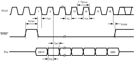 Figure 1. Serial Timing Diagram
7.7 Typical Characteristics
VREF = VA, fSCLK = 30 MHz, TA = 25°C, Input Code Range 3 to 252, unless otherwise stated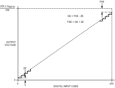 Figure 2. Input and Output Transfer Characteristic
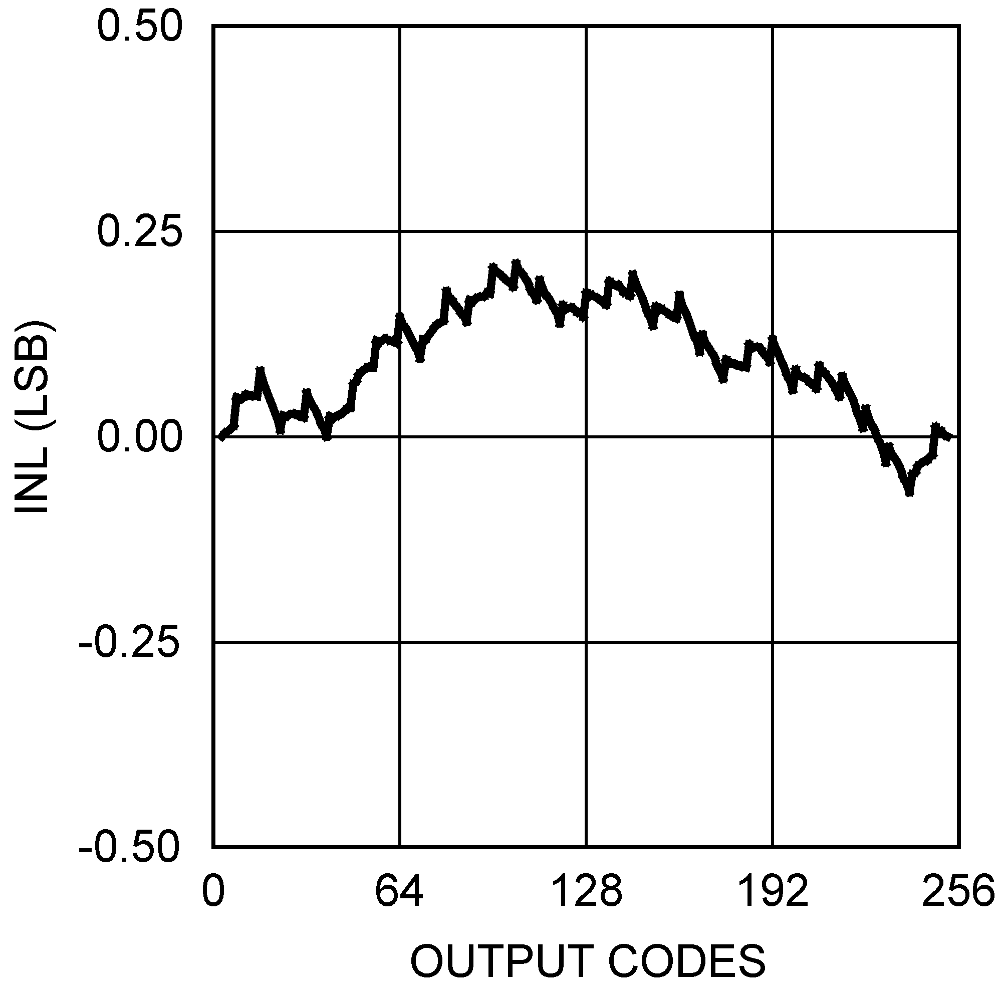 Figure 4. INL at VA = 5 V
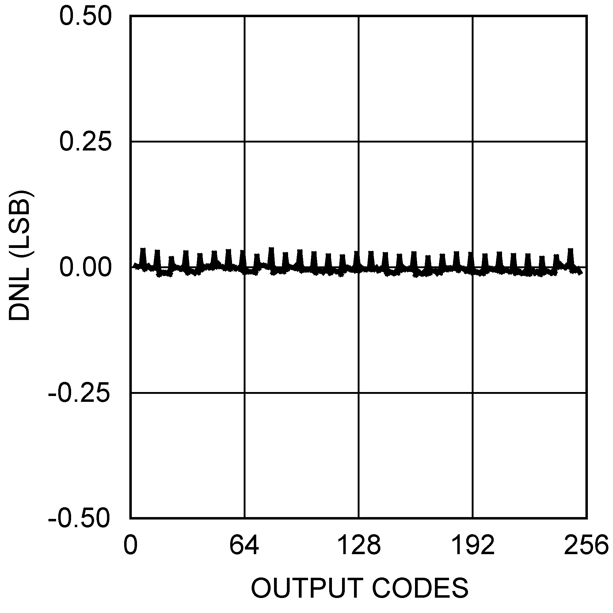 Figure 6. DNL at VA = 5 V
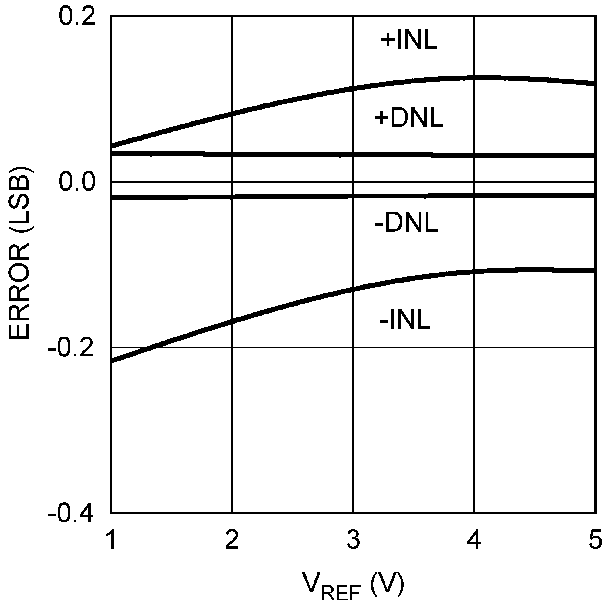 Figure 8. INL/DNL vs VREFIN at VA = 5 V
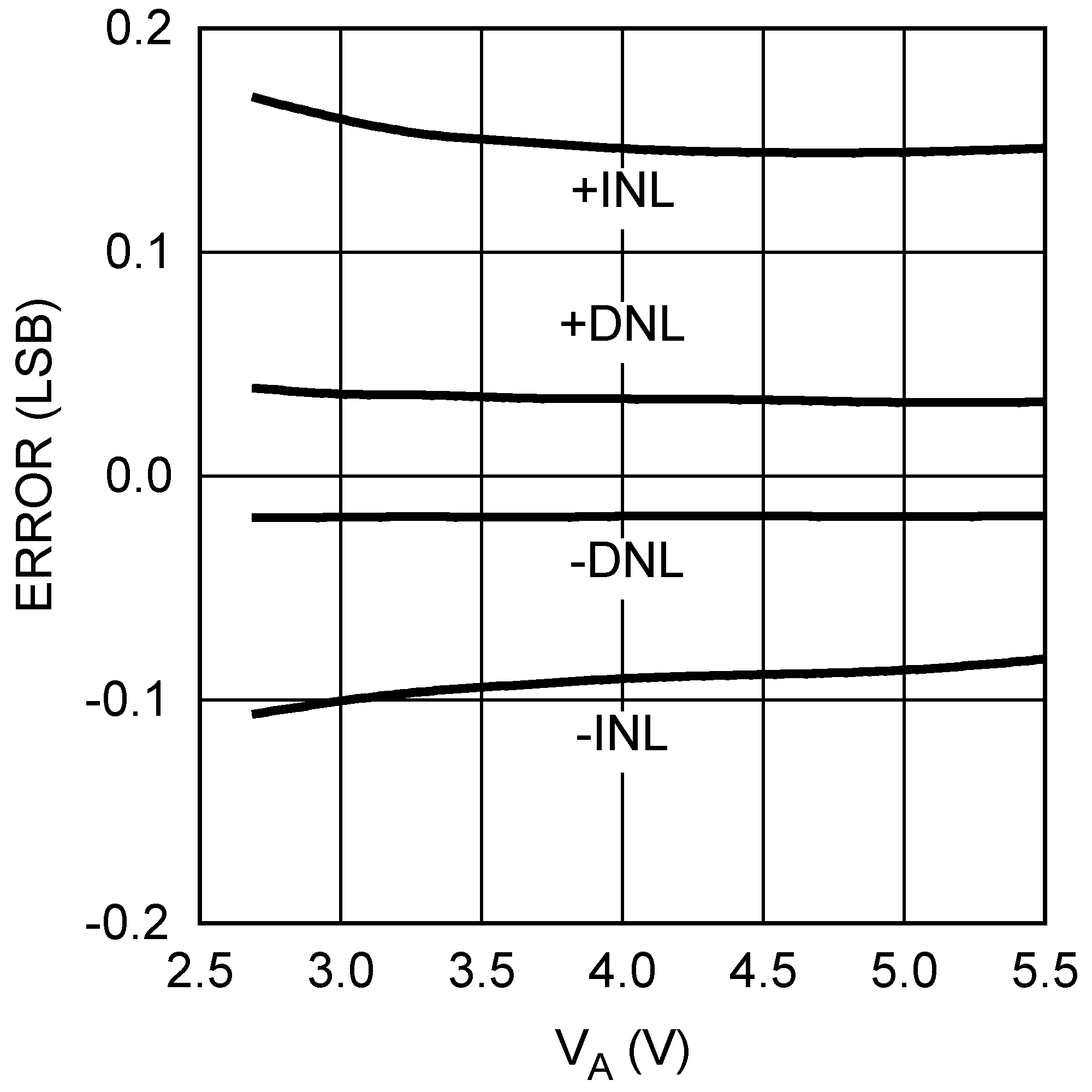 Figure 10. INL/DNL vs VA
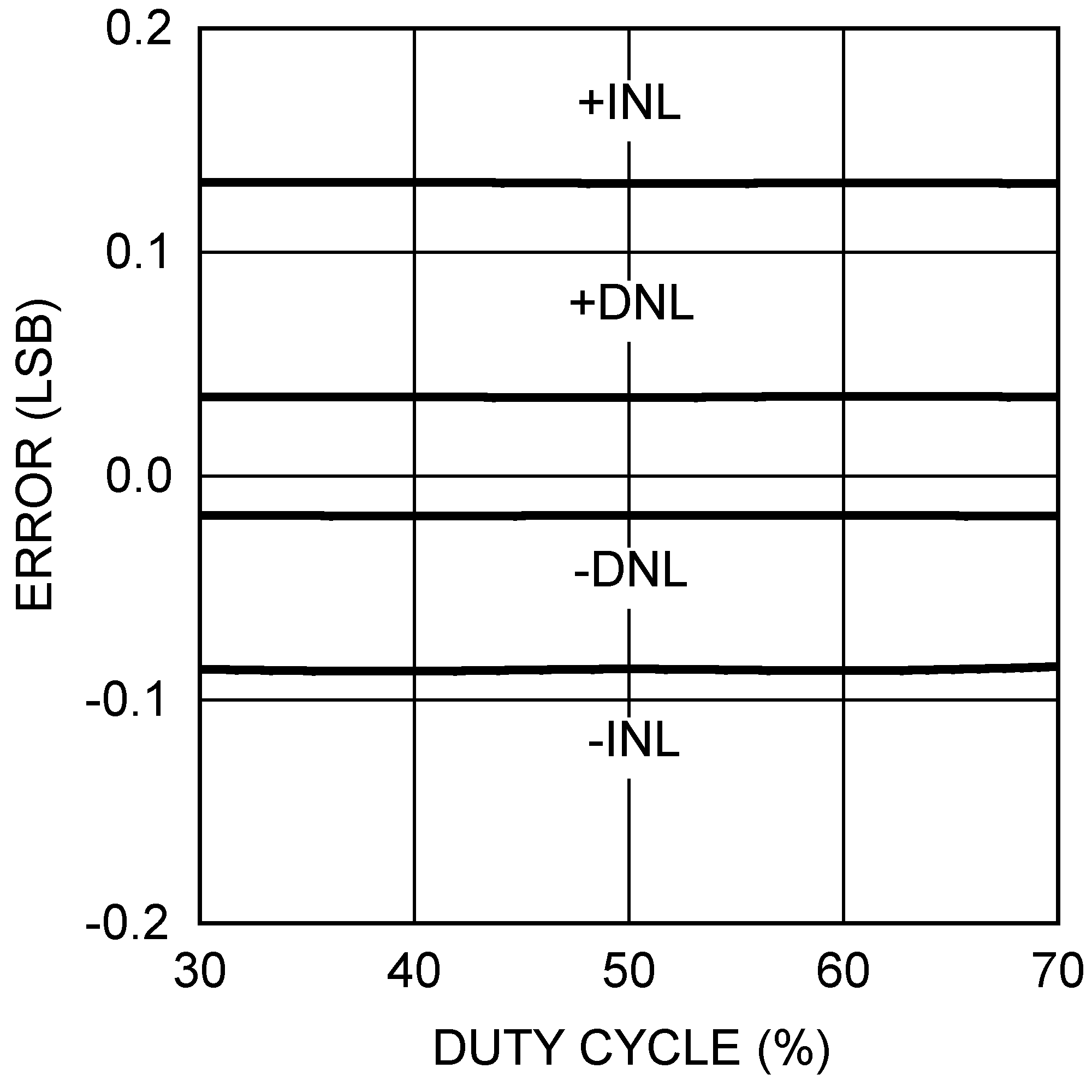 Figure 12. INL/DNL vs Clock Duty Cycle at VA = 5 V
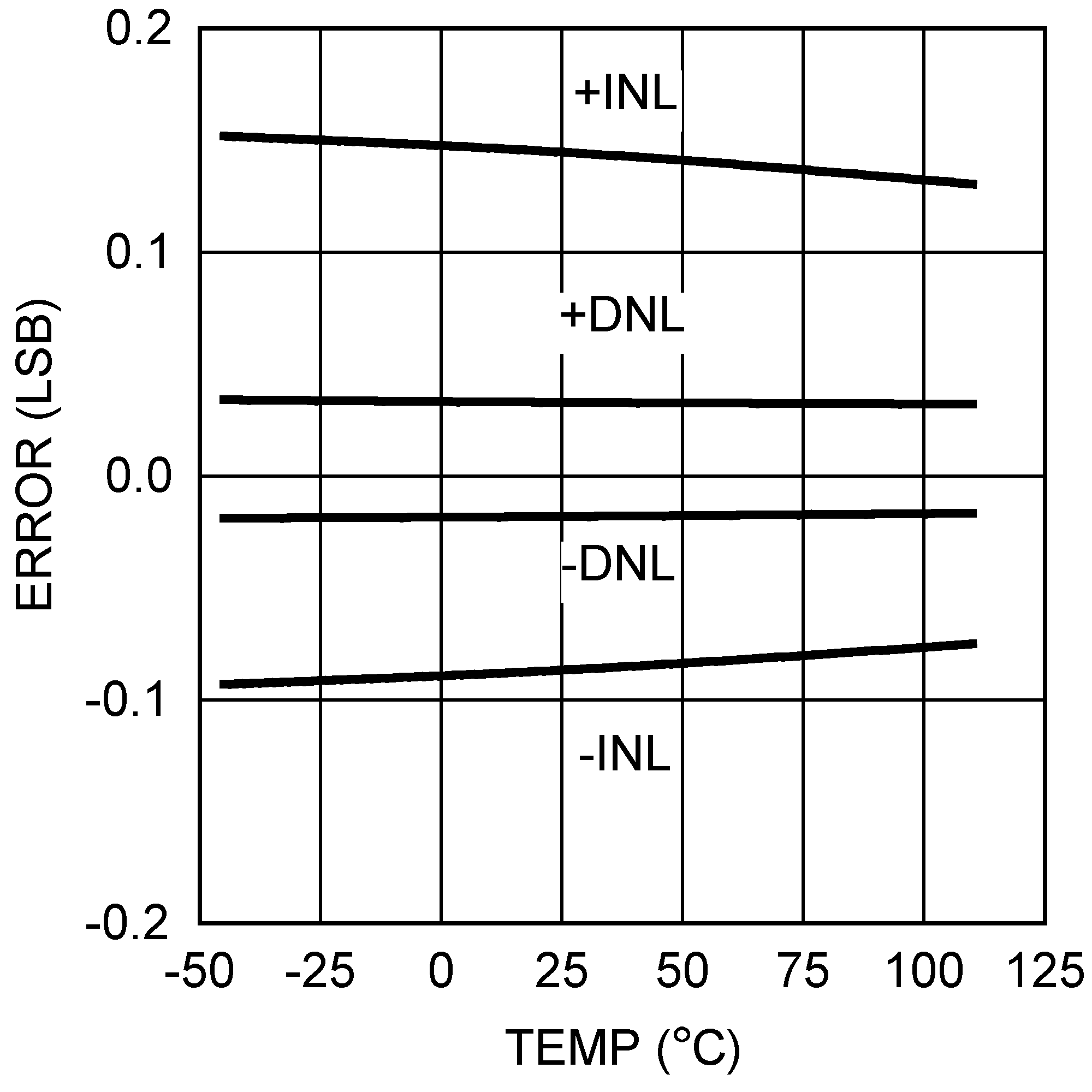 Figure 14. INL/DNL vs Temperature at VA = 5 V
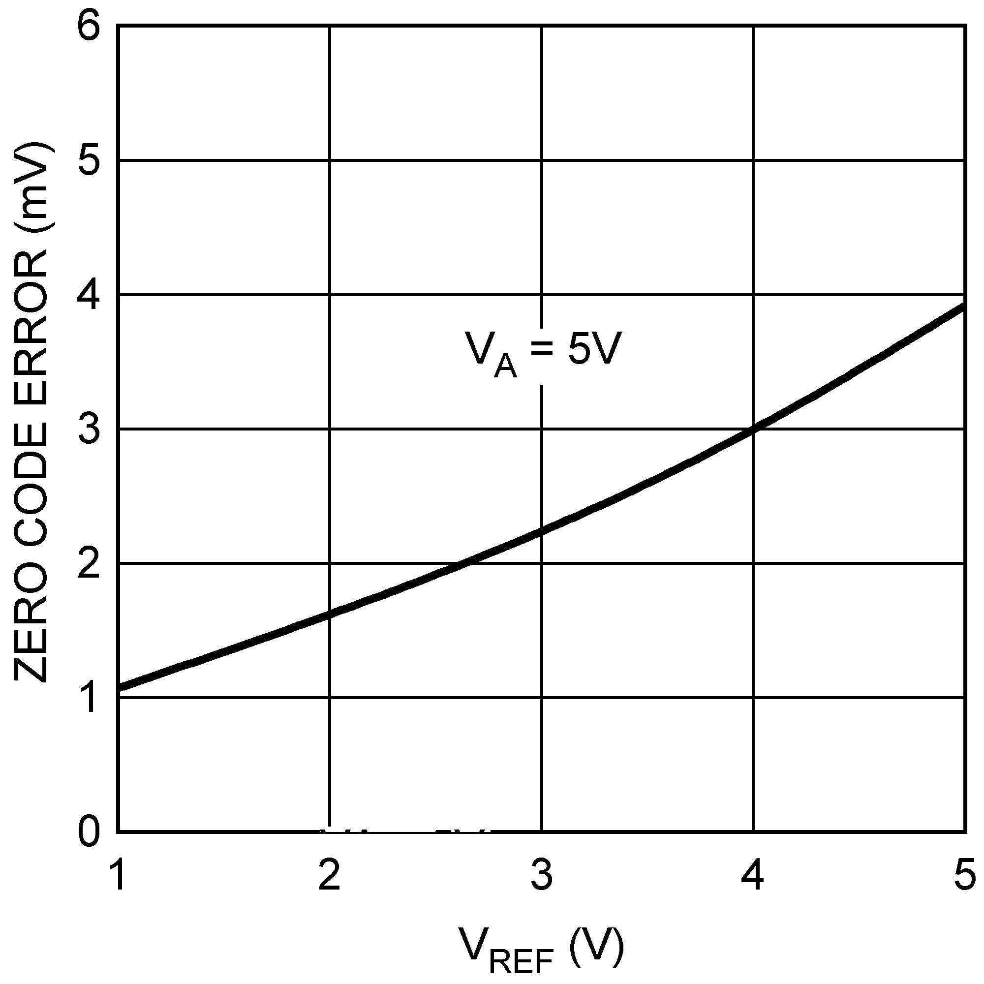 Figure 16. Zero Code Error vs VREFIN
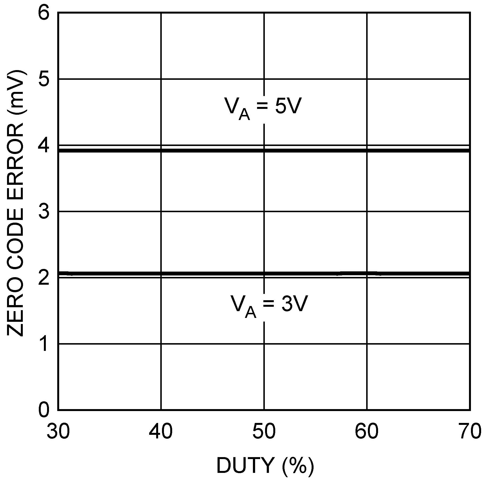 Figure 18. Zero Code Error vs Clock Duty Cycle
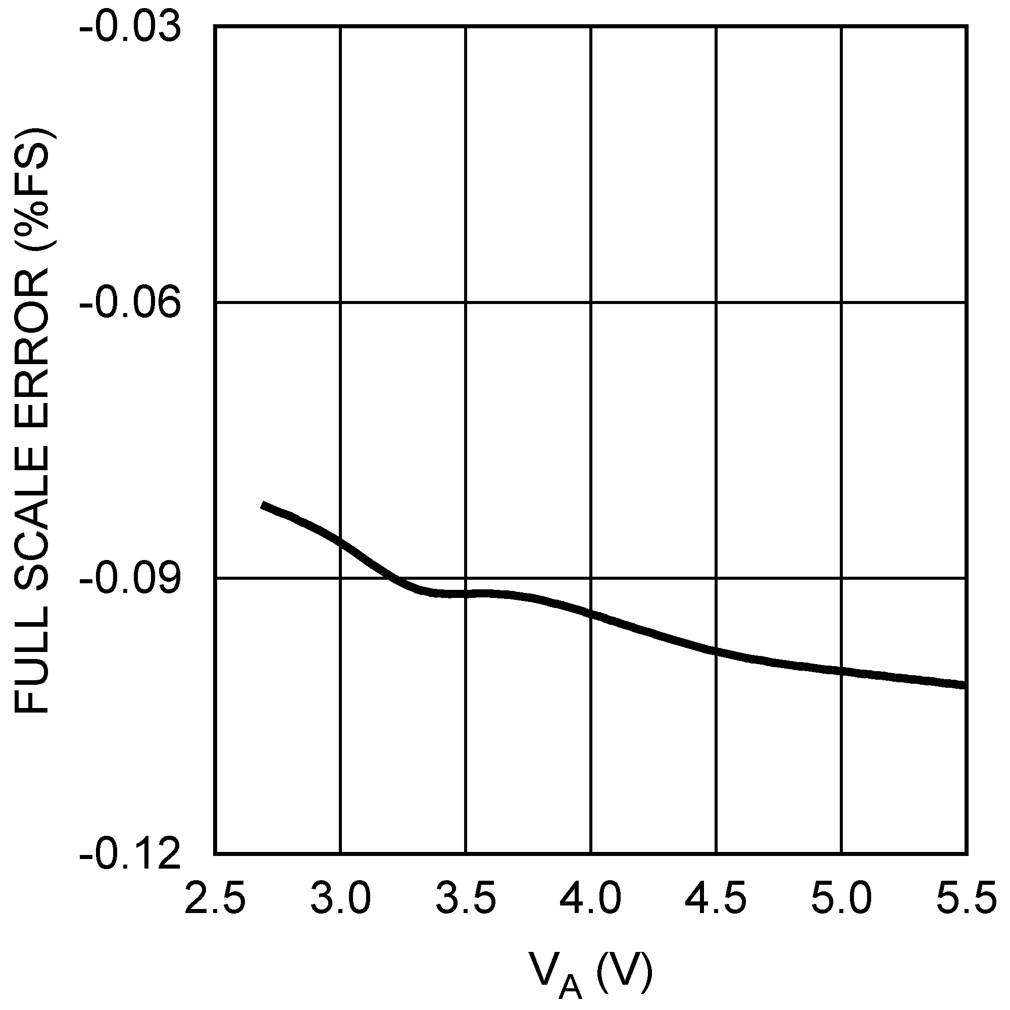 Figure 20. Full-Scale Error vs VA
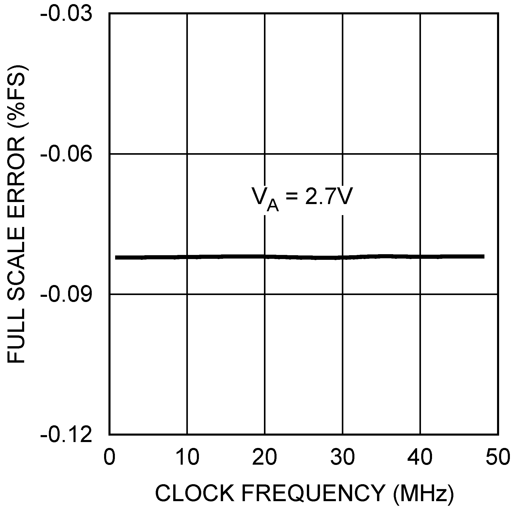 Figure 22. Full-Scale Error vs fSCLK
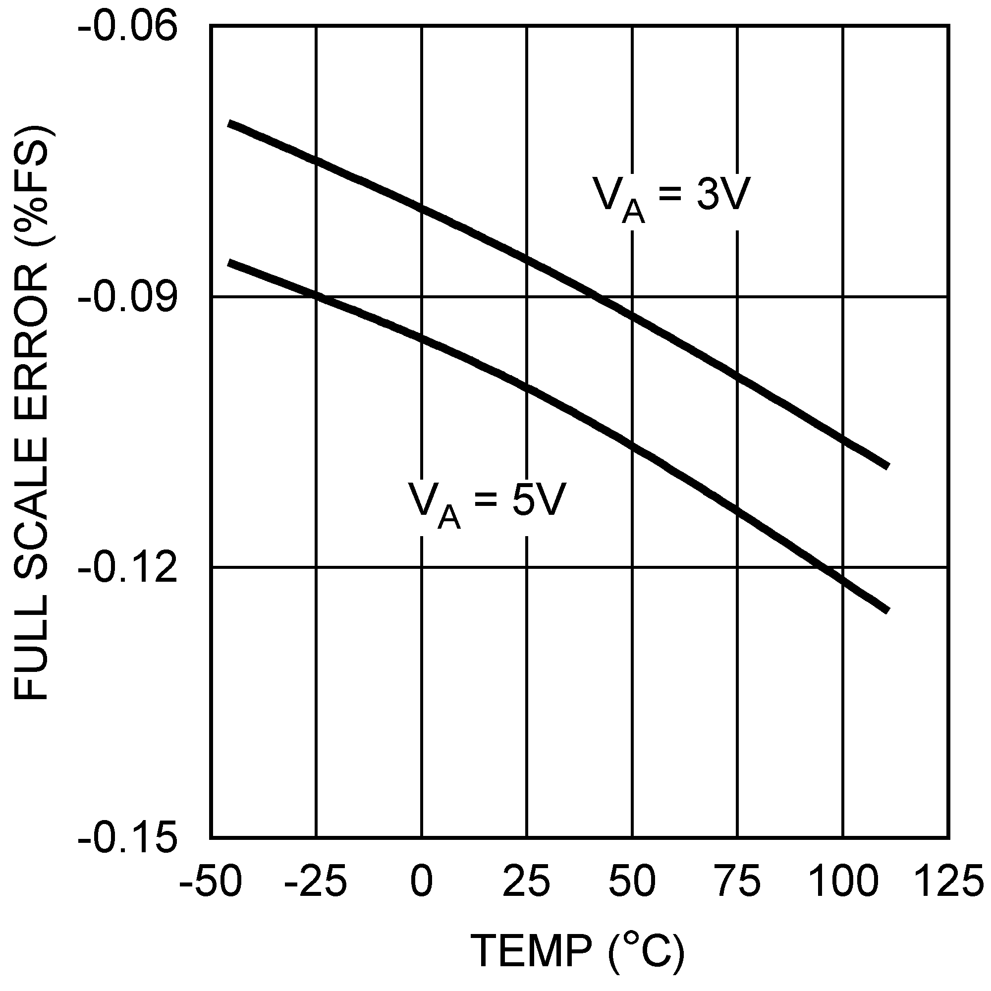 Figure 24. Full-Scale Error vs Temperature
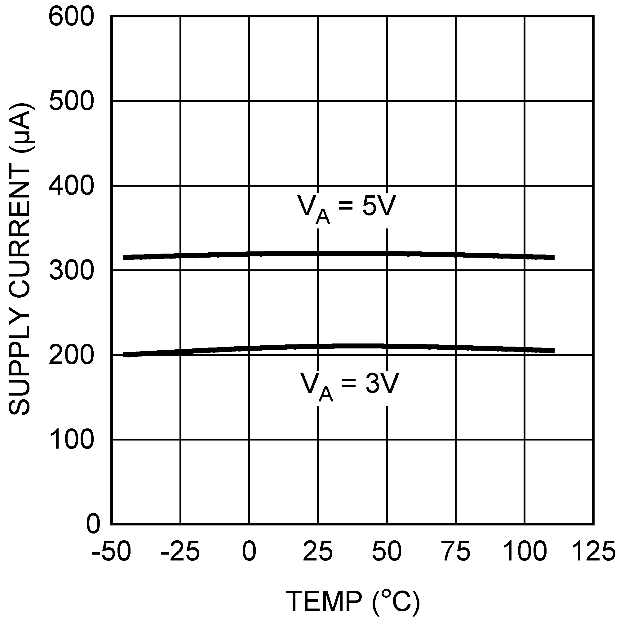 Figure 26. Supply Current vs Temperature
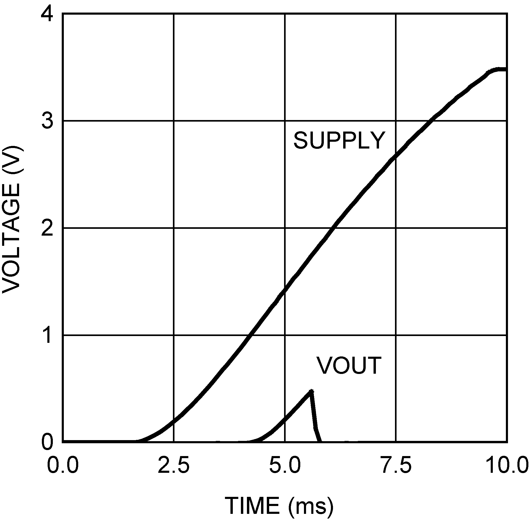 Figure 28. Power-On Reset
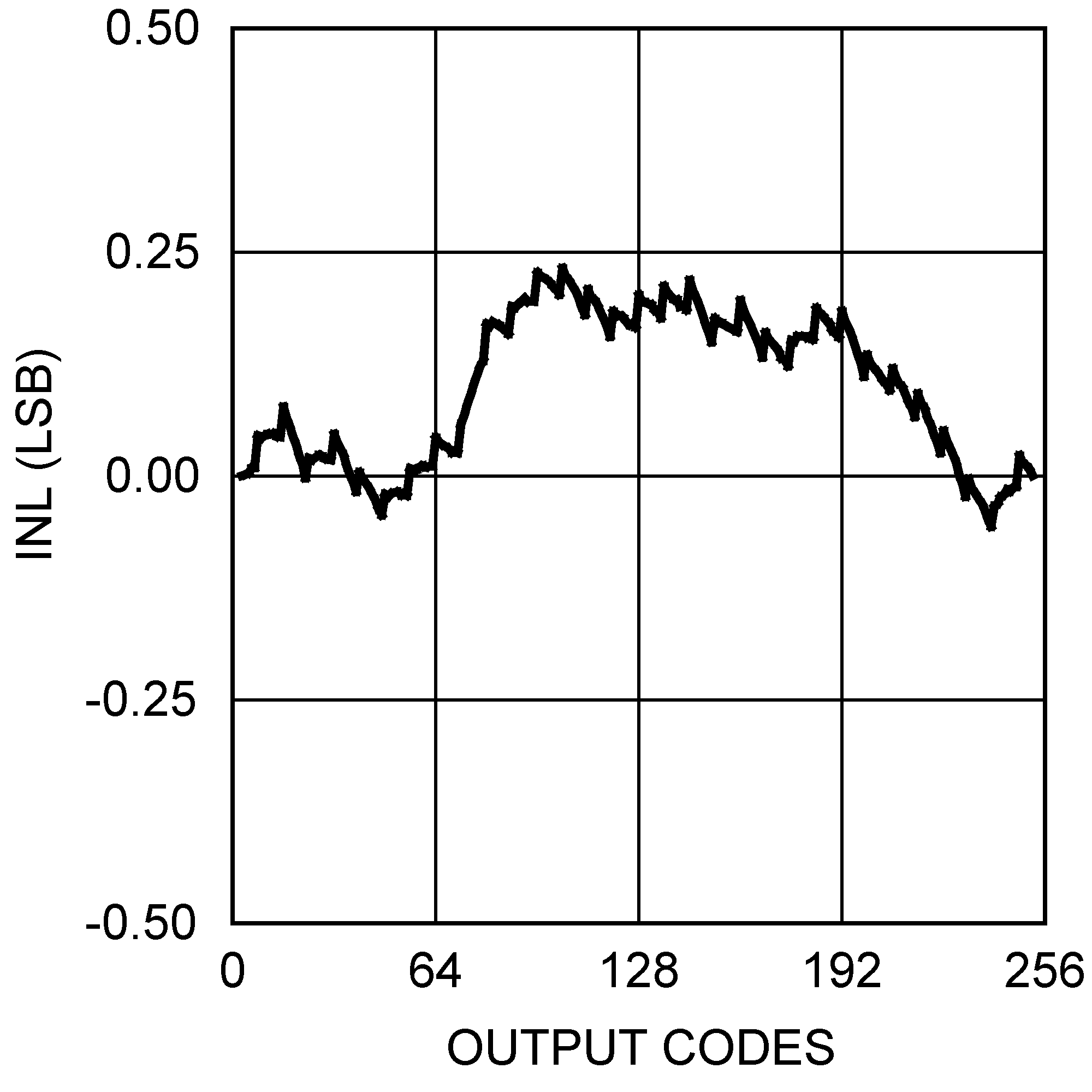
 Figure 5. DNL at VA = 3 V
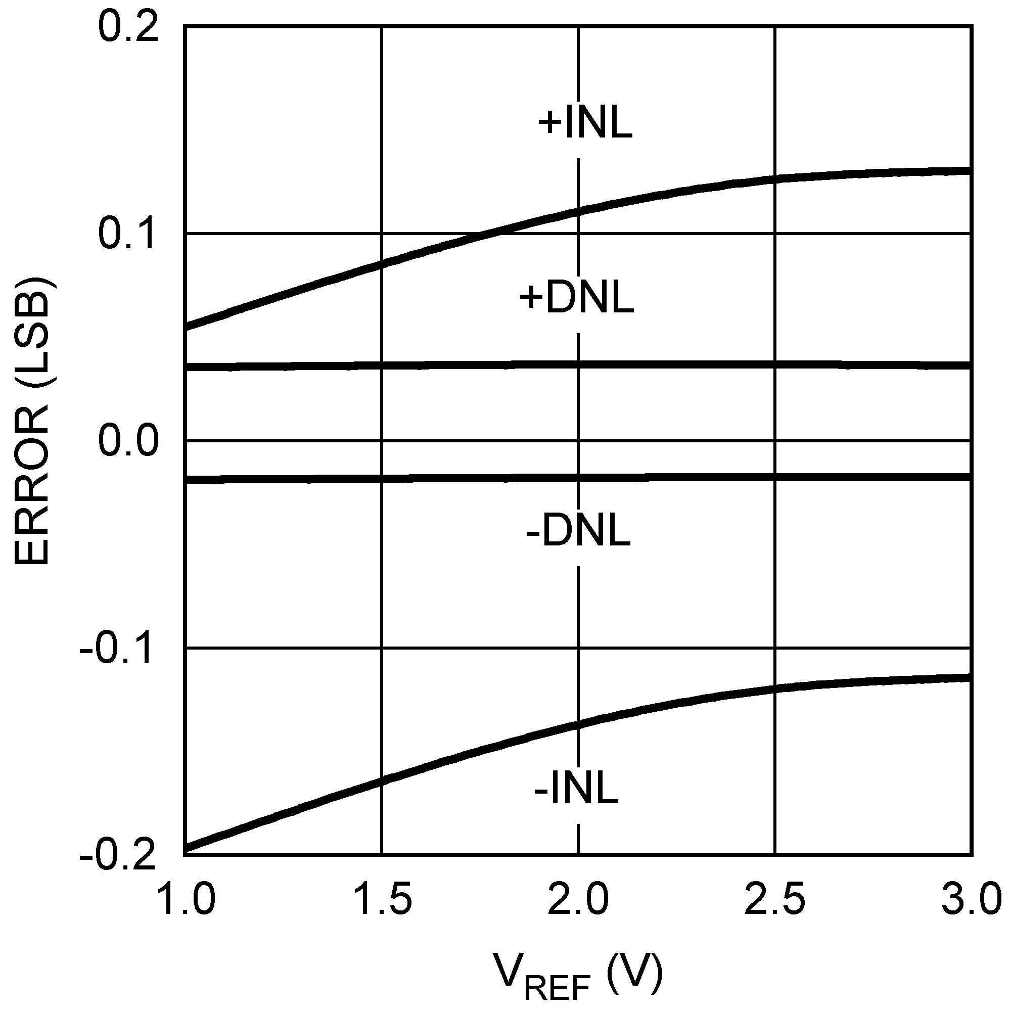 Figure 7. INL/DNL vs VREFIN at VA = 3 V
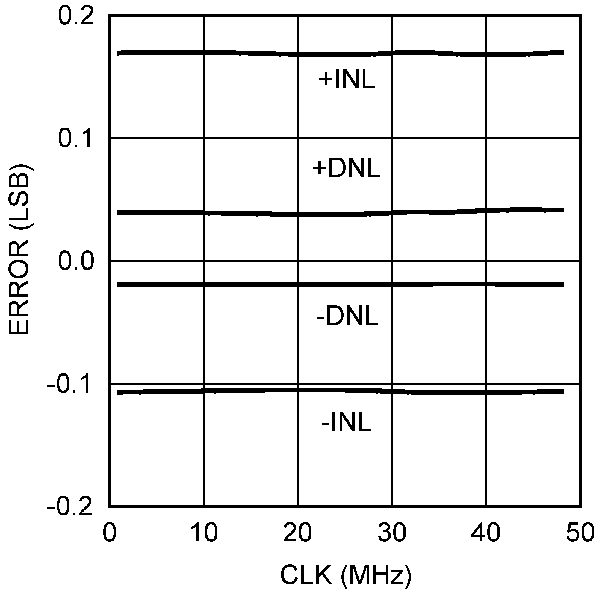 Figure 9. INL/DNL vs fSCLK at VA = 2.7 V
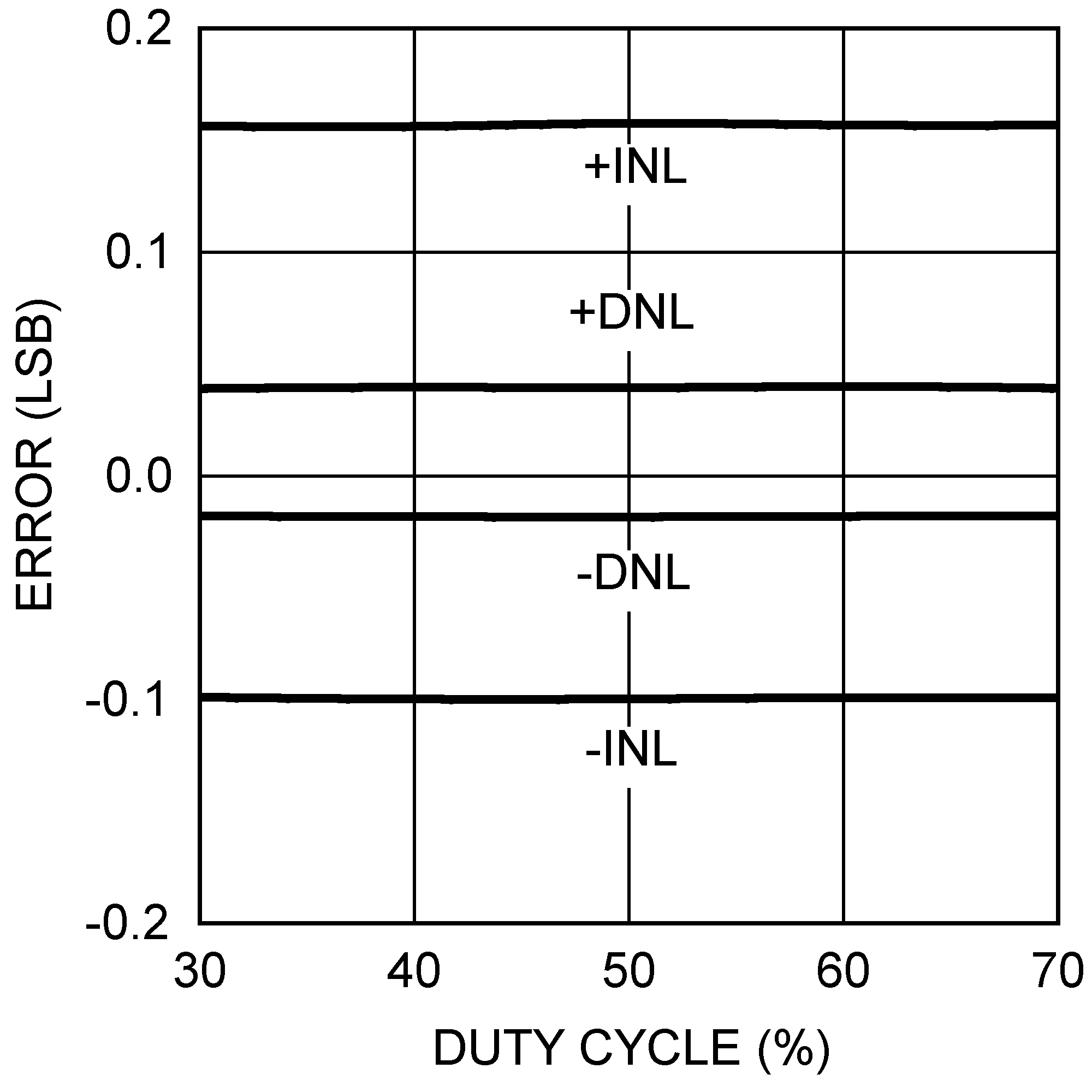 Figure 11. INL/DNL vs Clock Duty Cycle at VA = 3 V
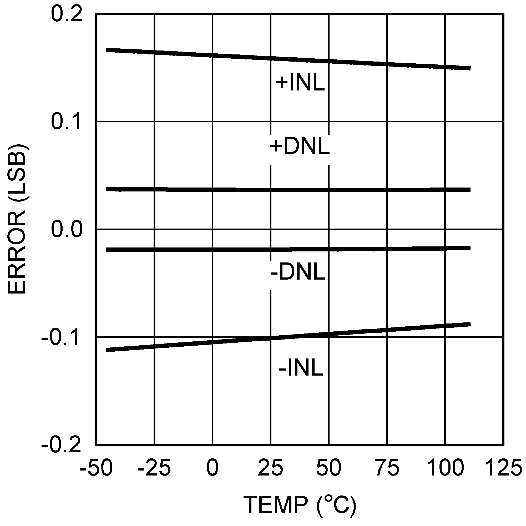 Figure 13. INL/DNL vs Temperature at VA = 3 V
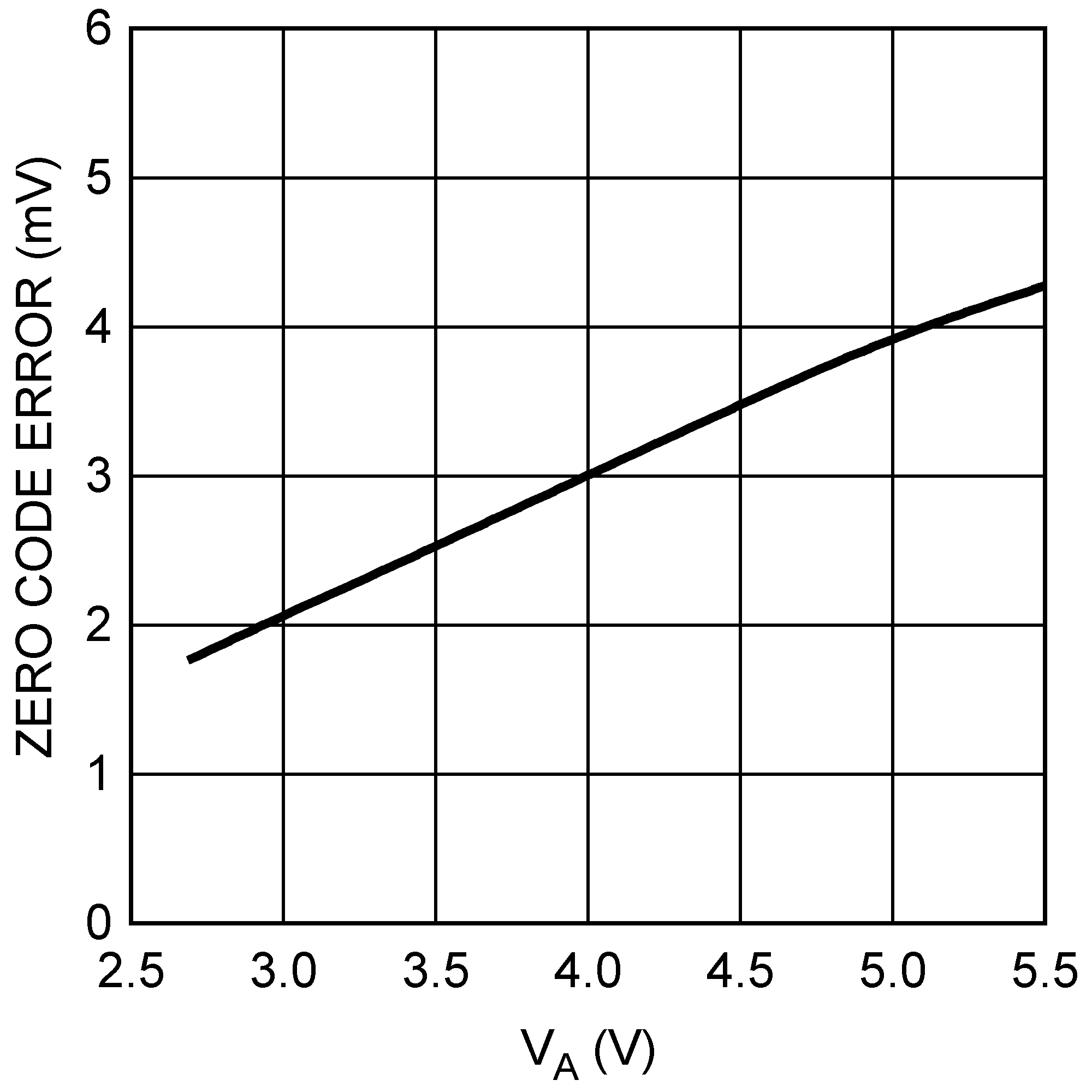 Figure 15. Zero Code Error vs VA
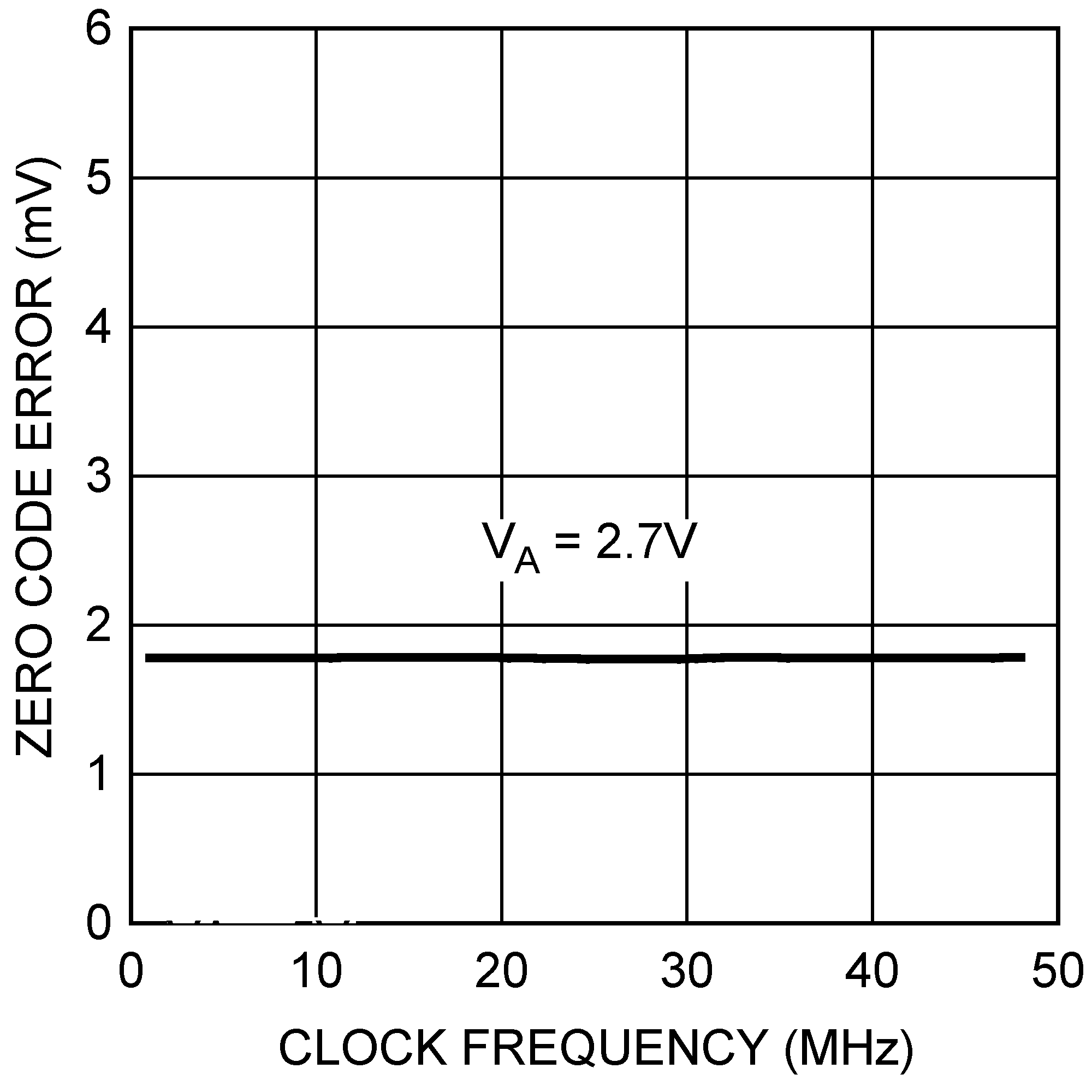 Figure 17. Zero Code Error vs fSCLK
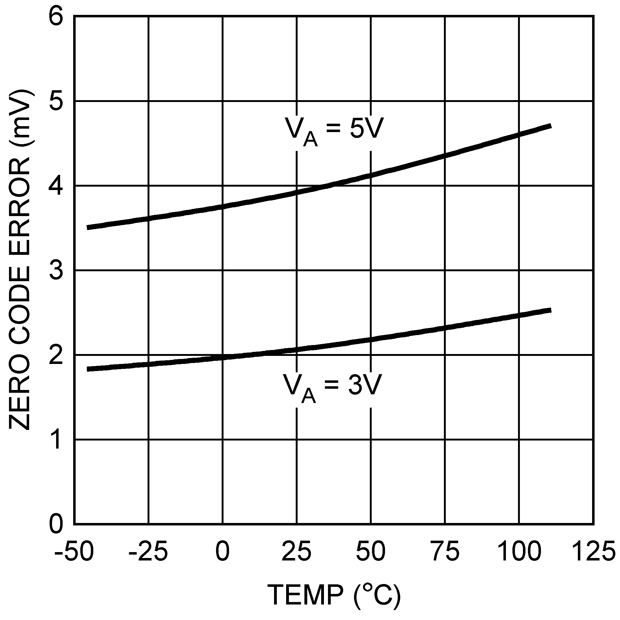 Figure 19. Zero Code Error vs Temperature
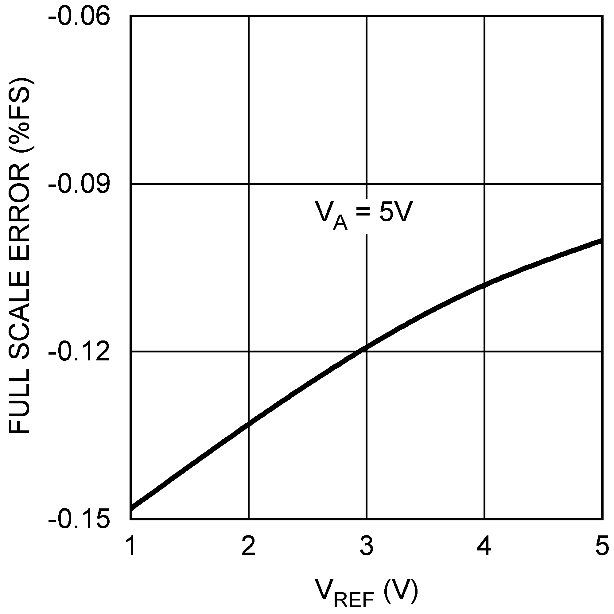 Figure 21. Full-Scale Error vs VREFIN
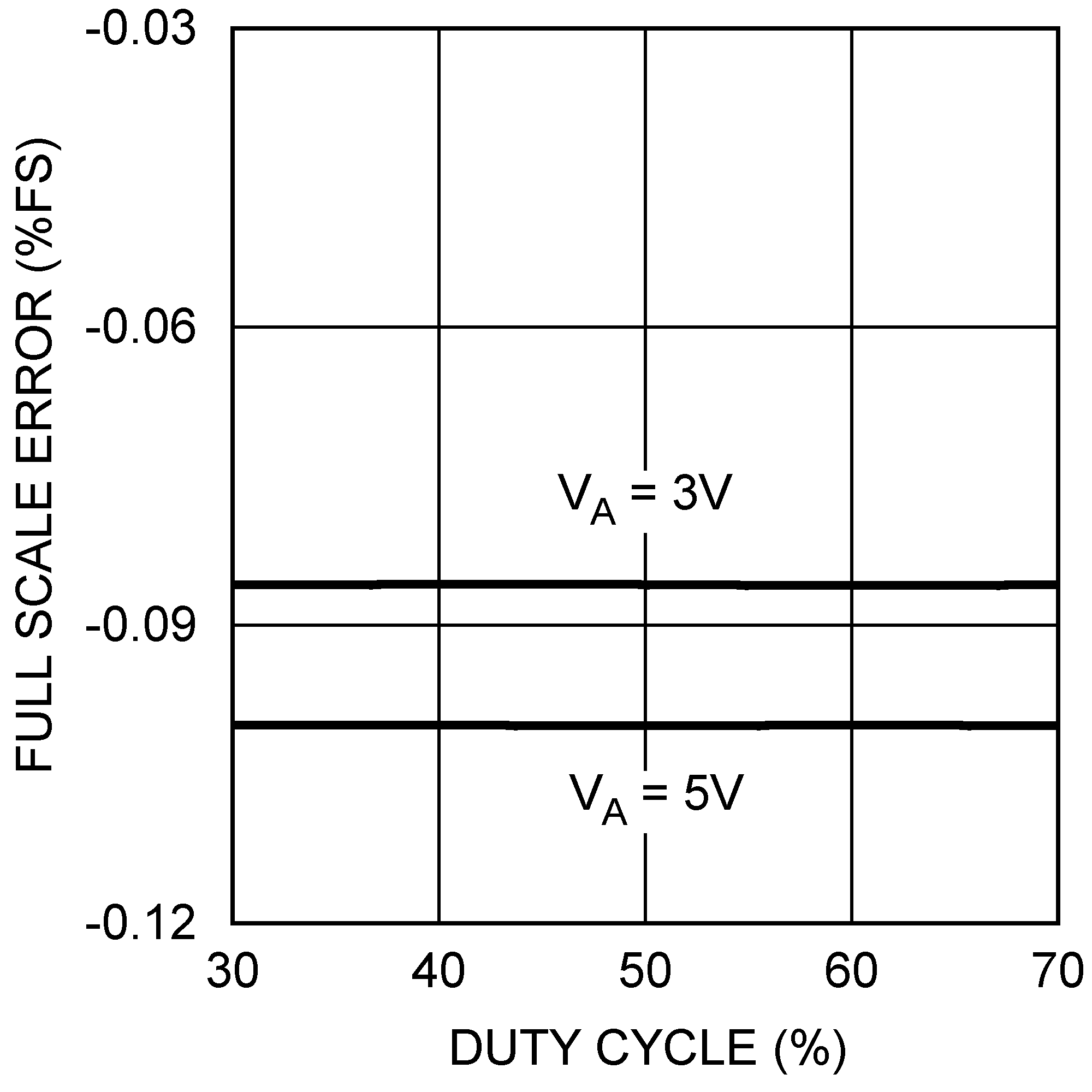 Figure 23. Full-Scale Error vs Clock Duty Cycle
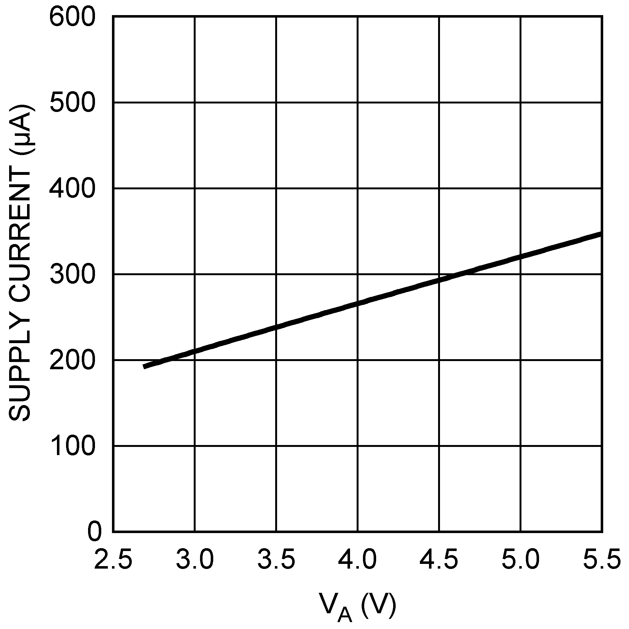 Figure 25. Supply Current vs VA
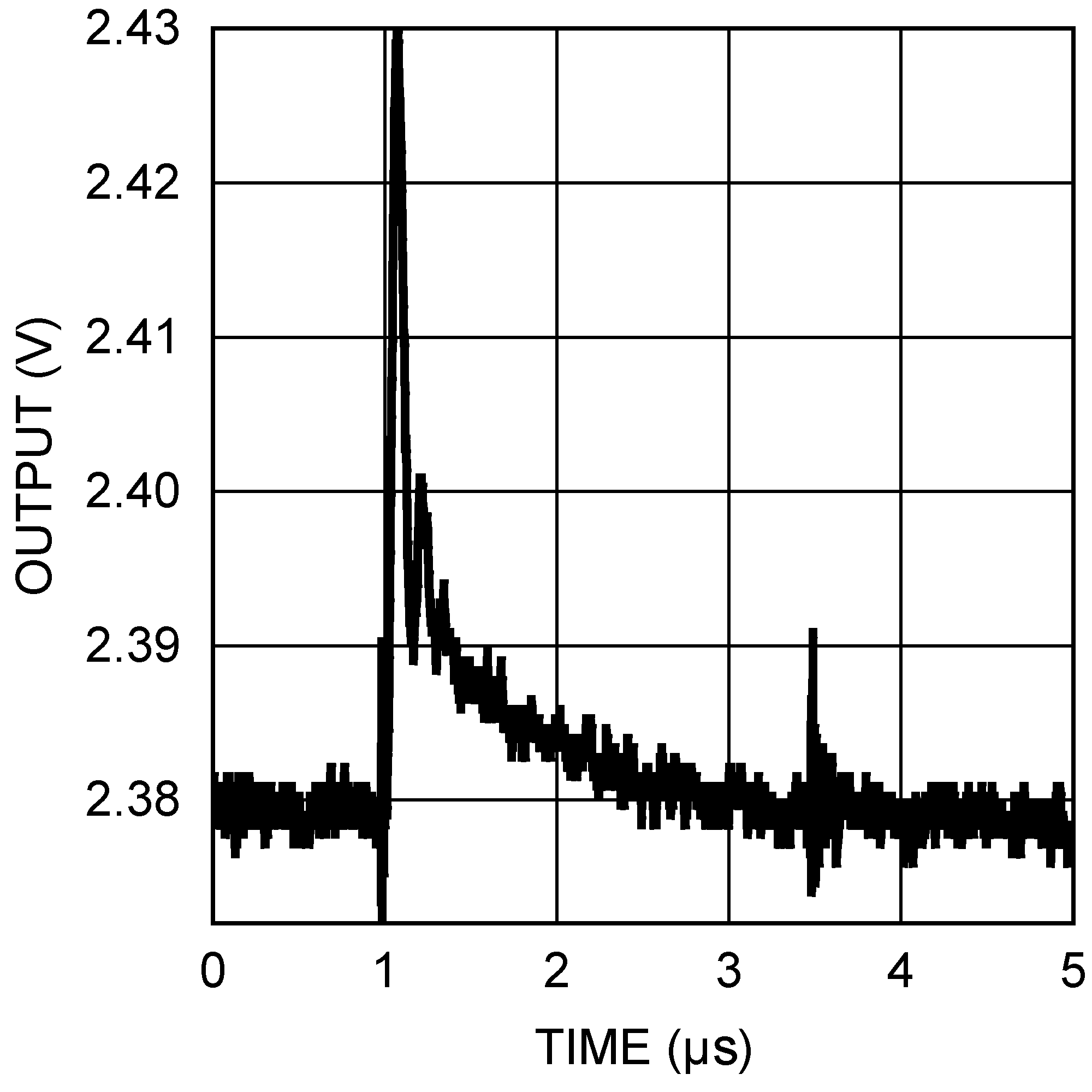 Figure 27. 5-V Glitch Response
8 Detailed Description
8.1 Overview
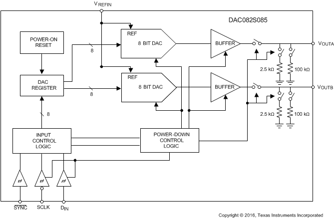
The DAC082S085 is fabricated on a CMOS process with an architecture that consists of switches and resistor strings that are followed by an output buffer.
8.2 Functional Block Diagram
8.2.1 Feature Description
8.2.1.1 DAC Architecture
The DAC082S085 is fabricated on a CMOS process with an architecture that consists of switches and resistor strings that are followed by an output buffer. The reference voltage is externally applied at VREFIN and is shared by both DACs.
For simplicity, a single resistor string is shown in Figure 29. This string consists of 256 equal valued resistors with a switch at each junction of two resistors, plus a switch to ground. The code loaded into the DAC register determines which switch is closed, connecting the proper node to the amplifier. The input coding is straight binary with an ideal output voltage calculated in Equation 1:
where
- D is the decimal equivalent of the binary code that is loaded into the DAC register. (D can take on any value between 0 and 255. This configuration ensures that the DAC is monotonic.)
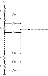 Figure 29. DAC Resistor String
8.2.1.2 Output Amplifiers
The output amplifiers are rail-to-rail, providing an output voltage range of 0 V to VA when the reference is VA. All amplifiers, even rail-to-rail types, exhibit a loss of linearity as the output approaches the supply rails (0 V and VA, in this case). For this reason, linearity is specified over less than the full output range of the DAC. However, if the reference is less than VA, there is only a loss in linearity in the lowest codes. The output capabilities of the amplifier are described in Electrical Characteristics.
The output amplifiers are capable of driving a load of 2 kΩ in parallel with 1500 pF to ground or to VA. The zero-code and full-scale outputs for given load currents are available in the Electrical Characteristics.
8.2.1.3 Reference Voltage
The DAC082S085 uses a single external reference that is shared by both channels. The reference pin, VREFIN, is not buffered and has an input impedance of 60 kΩ. TI recommends that VREFIN be driven by a voltage source with low output impedance. The reference voltage range is 1 V to VA, providing the widest possible output dynamic range.
8.2.1.4 Power-On Reset
The power-on reset circuit controls the output voltages of both DACs during power-up. Upon application of power, the DAC registers are filled with zeros and the output voltages are 0 V. The outputs remain at 0 V until a valid write sequence is made to the DAC.
8.3 Device Functional Modes
8.3.1 Power-Down Modes
The DAC082S085 has four power-down modes, two of which are identical. In power-down mode, the supply current drops to 20 µA at 3 V and 30 µA at 5 V. The DAC082S085 is set in power-down mode by setting OP1 and OP0 to 11. Because this mode powers down both DACs, the first two bits of the shift register are used to select different output terminations for the DAC outputs. Setting A1 and A0 to 00 or 11 causes the outputs to be tri-stated (a high impedance state). While setting A1 and A0 to 01 or 10 causes the outputs to be terminated by 2.5 kΩ or 100 kΩ to ground respectively (see Table 1).
Table 1. Power-Down Modes
| A1 | A0 | OP1 | OP0 | OPERATING MODE |
|---|---|---|---|---|
| 0 | 0 | 1 | 1 | High-Z outputs |
| 0 | 1 | 1 | 1 | 2.5 kΩ to GND |
| 1 | 0 | 1 | 1 | 100 kΩ to GND |
| 1 | 1 | 1 | 1 | High-Z outputs |
The bias generator, output amplifiers, resistor strings, and other linear circuitry are all shut down in any of the power-down modes. However, the contents of the DAC registers are unaffected when in power-down. Each DAC register maintains its value prior to the DAC082S085 being powered down unless it is changed during the write sequence which instructed it to recover from power down. Minimum power consumption is achieved in the power-down mode with SYNC and DIN idled low and SCLK disabled. The time to exit power-down (Wake-Up Time) is typically tWU µs as stated in Timing Requirements.
8.4 Programming
8.4.1 Serial Interface
The three-wire interface is compatible with SPI™, QSPI, and MICROWIRE, as well as most DSPs and operates at clock rates up to 40 MHz. See Figure 1 for information on a write sequence.
A write sequence begins by bringing the SYNC line low. Once SYNC is low, the data on the DIN line is clocked into the 16-bit serial input register on the falling edges of SCLK. To avoid misclocking data into the shift register, it is critical that SYNC not be brought low simultaneously with a falling edge of SCLK (see Figure 1). On the 16th falling clock edge, the last data bit is clocked in and the programmed function (a change in the DAC channel address, mode of operation or register contents) is executed. At this point the SYNC line may be kept low or brought high. Any data and clock pusles after the 16th falling clock edge are ignored. In either case, SYNC must be brought high for the minimum specified time before the next write sequence is initiated with a falling edge of SYNC.
Because the SYNC and DIN buffers draw more current when they are high, they must be idled low between write sequences to minimize power consumption.
8.4.2 Input Shift Register
The input shift register, Figure 30, has sixteen bits. The first bit must be set to 0 and the second bit is an address bit. The address bit determines whether the register data is for DAC A or DAC B. This bit is followed by two bits that determine the mode of operation (writing to a DAC register without updating the outputs of both DACs, writing to a DAC register and updating the outputs of both DACs, writing to the register of both DACs and updating their outputs, or powering down both outputs). The final twelve bits of the shift register are the data bits. The data format is straight binary (MSB first, LSB last), with all 0s corresponding to an output of 0 V and all 1s corresponding to a full-scale output of VREFIN – 1 LSB. The contents of the serial input register are transferred to the DAC register on the sixteenth falling edge of SCLK. See Figure 1.
 Figure 30. Input Register Contents
Normally, the SYNC line is kept low for at least 16 falling edges of SCLK and the DAC is updated on the 16th SCLK falling edge. However, if SYNC is brought high before the 16th falling edge, the data transfer to the shift register is aborted and the write sequence is invalid. Under this condition, the DAC register is not updated and there is no change in the mode of operation or in the DAC output voltages.
8.4.3 DSP and Microprocessor Interfacing
Interfacing the DAC082S085 to microprocessors and DSPs is quite simple. The following guidelines are offered to hasten the design process.
8.4.3.1 ADSP-2101/ADSP2103 Interfacing
Figure 31 shows a serial interface between the DAC082S085 and the ADSP-2101/ADSP2103. The DSP must be set to operate in the SPORT Transmit Alternate Framing Mode. It is programmed through the SPORT control register and must be configured for Internal Clock Operation, Active Low Framing and 16-bit Word Length. Transmission is started by writing a word to the TX register after the SPORT mode has been enabled.
 Figure 31. ADSP-2101/2103 Interface
8.4.3.2 80C51/80L51 Interface
A serial interface between the DAC082S085 and the 80C51/80L51 microcontroller is shown in Figure 32. The SYNC signal comes from a bit-programmable pin on the microcontroller. The example shown here uses port line P3.3. This line is taken low when data is transmitted to the DAC082S085. Because the 80C51/80L51 transmits
8-bit bytes, only eight falling clock edges occur in the transmit cycle. To load data into the DAC, the P3.3 line must be left low after the first eight bits are transmitted. A second write cycle is initiated to transmit the second byte of data, after which port line P3.3 is brought high. The 80C51/80L51 transmit routine must recognize that the 80C51/80L51 transmits data with the LSB first while the DAC082S085 requires data with the MSB first.
 Figure 32. 80C51/80L51 Interface
8.4.3.3 68HC11 Interface
A serial interface between the DAC082S085 and the 68HC11 microcontroller is shown in Figure 33. The SYNC line of the DAC082S085 is driven from a port line (PC7 in the figure), similar to the 80C51/80L51.
The 68HC11 must be configured with its CPOL bit as a zero and its CPHA bit as a one. This configuration causes data on the MOSI output to be valid on the falling edge of SCLK. PC7 is taken low to transmit data to the DAC. The 68HC11 transmits data in 8-bit bytes with eight falling clock edges. Data is transmitted with the MSB first. PC7 must remain low after the first eight bits are transferred. A second write cycle is initiated to transmit the second byte of data to the DAC, after which PC7 must be raised to end the write sequence.
 Figure 33. 68HC11 Interface
8.4.3.4 Microwire Interface
Figure 34 shows an interface between a Microwire-compatible device and the DAC082S085. Data is clocked out on the rising edges of the SK signal. As a result, the SK of the Microwire device must be inverted before driving the SCLK of the DAC082S085.
 Figure 34. Microwire Interface
9 Application and Implementation
NOTE
Information in the following applications sections is not part of the TI component specification, and TI does not warrant its accuracy or completeness. TI’s customers are responsible for determining suitability of components for their purposes. Customers should validate and test their design implementation to confirm system functionality.
9.1 Application Information
The DAC082S085 is designed for single-supply operation and thus has a unipolar output. However, a bipolar output may be obtained with the circuit in Figure 35. This circuit provides an output voltage range of ±5 V. A rail-to-rail amplifier must be used if the amplifier supplies are limited to ±5 V.
9.2 Typical Application
9.2.1 Bipolar Operation
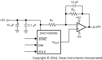 Figure 35. Bipolar Operation
9.2.1.1 Design Requirements
- The DAC082S085 uses a single supply.
- The output is required to be bipolar with a voltage range of ±5 V.
- Dual supplies are used for the output amplifier.
9.2.1.2 Detailed Design Procedure
The output voltage of this circuit for any code is found to be
where
- D is the input code in decimal form (With VA = 5 V and R1 = R2)
Table 2 lists the rail-to-rail amplifiers suitable for this application.
Table 2. Some Rail-to-Rail Amplifiers
| AMP | PKGS | TYP VOS | TYP ISUPPLY |
|---|---|---|---|
| LMC7111 | 8-pin PDIP, 5-pin SOT-23 | 0.9 mV | 25 µA |
| LM7301 | 8-pin SO, 5-pin SOT-23 | 0.03 mV | 620 µA |
| LM8261 | 5-pin SOT-23 | 0.7 mV | 1 mA |
9.2.1.3 Application Curve
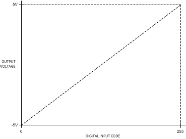 Figure 36. Bipolar Input / Output Transfer Characteristic
10 Power Supply Recommendations
While the simplicity of the DAC082S085 implies ease of use, it is important to recognize that the path from the reference input (VREFIN) to the VOUTs has essentially zero Power Supply Rejection Ratio (PSRR). Therefore, it is necessary to provide a noise-free supply voltage to VREFIN. To use the full dynamic range of the DAC082S085, the supply pin (VA) and VREFIN can be connected together and share the same supply voltage.
10.1 Using References as Power Supplies
Because the DAC082S085 consumes very little power, a reference source may be used as the reference input or the supply voltage. The advantages of using a reference source over a voltage regulator are accuracy and stability. Some low noise regulators can also be used. Listed below are a few reference and power supply options for the DAC082S085.
10.1.1 LM4130
The LM4130, with its 0.05% accuracy over temperature, is a good choice as a reference source for the DAC082S085. The 4.096-V version is useful if a 0 to 4.095-V output range is desirable or acceptable. Bypassing the LM4130 VIN pin with a 0.1-µF capacitor and the VOUT pin with a 2.2-µF capacitor improves stability and reduces output noise. The LM4130 comes in a space-saving, 5-pin SOT-23.
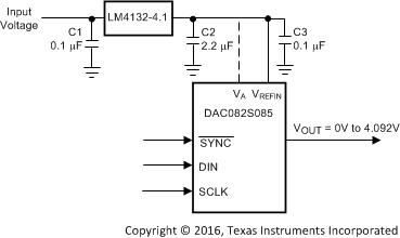 Figure 37. The LM4130 as a Power Supply
10.1.2 LM4050
Available with accuracy of 0.44%, the LM4050 shunt reference is also a good choice as a reference for the DAC082S085. It is available in 4.096-V and 5-V versions and comes in a space-saving, 3-pin SOT-23.
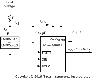 Figure 38. The LM4050 as a Power Supply
The minimum resistor value in the circuit of Figure 38 must be chosen such that the maximum current through the LM4050 does not exceed its 15-mA rating. The conditions for maximum current include the input voltage at its maximum, the LM4050 voltage at its minimum, and the DAC082S085 drawing zero current. The maximum resistor value must allow the LM4050 to draw more than its minimum current for regulation plus the maximum DAC082S085 current in full operation. The conditions for minimum current include the input voltage at its minimum, the LM4050 voltage at its maximum, the resistor value at its maximum due to tolerance, and the DAC082S085 draws its maximum current. These conditions can be summarized in Equation 4 and Equation 5:
where
- VZ(min) and VZ(max) are the nominal LM4050 output voltages ± the LM4050 output tolerance over temperature
- IZ(max) is the maximum allowable current through the LM4050
- IZ(min) is the minimum current required by the LM4050 for proper regulation
- IDAC(max) is the maximum DAC082S085 supply current
10.1.3 LP3985
The LP3985 is a low-noise, ultra-low dropout voltage regulator with a 3% accuracy over temperature. It is a good choice for applications that do not require a precision reference for the DAC082S085. It comes in 3-V, 3.3-V, and 5-V versions, among others, and sports a low 30-µV noise specification at low frequencies. Because low frequency noise is relatively difficult to filter, this specification could be important for some applications. The LP3985 comes in a space-saving, 5-pin SOT-23 and 5-bump DSBGA packages.
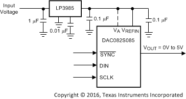 Figure 39. Using the LP3985 Regulator
An input capacitance of 1 µF without any ESR requirement is required at the LP3985 input, while a 1-µF ceramic capacitor with an ESR requirement of 5 mΩ to 500 mΩ is required at the output. Careful interpretation and understanding of the capacitor specification is required to ensure correct device operation.
10.1.4 LP2980
The LP2980 is an ultra-low dropout regulator with a 0.5% or 1% accuracy over temperature, depending upon grade. It is available in 3-V, 3.3-V, and 5-V versions, among others.
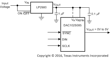 Figure 40. Using the LP2980 Regulator
Like any low dropout regulator, the LP2980 requires an output capacitor for loop stability. This output capacitor must be at least 1-µF over temperature, but values of 2.2 µF or more provide even better performance. The ESR of this capacitor must be within the range specified in the LP2980 data sheet. Surface-mount solid tantalum capacitors offer a good combination of small size and ESR. Ceramic capacitors are attractive due to their small size but generally have ESR values that are too low for use with the LP2980. Aluminum electrolytic capacitors are typically not a good choice due to their large size and have ESR values that may be too high at low temperatures.
11 Layout
11.1 Layout Guidelines
For best accuracy and minimum noise, the printed-circuit board containing the DAC082S085 must have separate analog and digital areas. The areas are defined by the locations of the analog and digital power planes. Both of these planes must be placed in the same board layer. There should be a single ground plane. A single ground plane is preferred if digital return current does not flow through the analog ground area. Frequently a single ground plane design uses a fencing technique to prevent the mixing of analog and digital ground current. Separate ground planes must only be used when the fencing technique is inadequate. The separate ground planes must be connected in one place, preferably near the DAC082S085. Take special care to ensure that digital signals with fast edge rates do not pass over split ground planes. They must always have a continuous return path below their traces.
The DAC082S085 power supply must be bypassed with a 10-µF and a 0.1-µF capacitor as close as possible to the device with the 0.1 µF right at the device supply pin. The 10-µF capacitor must be a tantalum type and the 0.1-µF capacitor must be a low ESL, low ESR type. The power supply for the DAC082S085 must only be used for analog circuits.
Avoid crossover of analog and digital signals and keep the clock and data lines on the component side of the board. The clock and data lines must have controlled impedances.
11.2 Layout Example
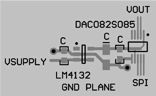 Figure 41. DAC082S085 Layout Example
12 Device and Documentation Support
12.1 Device Support
12.1.1 Device Nomenclature
12.1.1.1 Specification Definitions
DIFFERENTIAL NON-LINEARITY (DNL) is the measure of the maximum deviation from the ideal step size of 1 LSB, which is VREF / 256 = VA / 256.
DAC-to-DAC CROSSTALK is the glitch impulse transferred to a DAC output in response to a full-scale change in the output of another DAC.
DIGITAL CROSSTALK is the glitch impulse transferred to a DAC output at mid-scale in response to a full-scale change in the input register of another DAC.
DIGITAL FEEDTHROUGH is a measure of the energy injected into the analog output of the DAC from the digital inputs when the DAC outputs are not updated. It is measured with a full-scale code change on the data bus.
FULL-SCALE ERROR is the difference between the actual output voltage with a full scale code (FFFh) loaded into the DAC and the value of VA × 255 / 256.
GAIN ERROR is the deviation from the ideal slope of the transfer function. It can be calculated from Zero and Full-Scale Errors as GE = FSE – ZE, where GE is Gain error, FSE is Full-Scale Error and ZE is Zero Error.
GLITCH IMPULSE is the energy injected into the analog output when the input code to the DAC register changes. It is specified as the area of the glitch in nanovolt-seconds.
INTEGRAL NON-LINEARITY (INL) is a measure of the deviation of each individual code from a straight line through the input to output transfer function. The deviation of any given code from this straight line is measured from the center of that code value. The end point method is used. INL for this product is specified over a limited range, per the electrical tables.
LEAST SIGNIFICANT BIT (LSB) is the bit that has the smallest value or weight of all bits in a word. This value is
where
- VREF is the supply voltage for this product
- n is the DAC resolution in bits, which is 8 for the DAC082S085
MAXIMUM LOAD CAPACITANCE is the maximum capacitance that can be driven by the DAC with output stability maintained.
MONOTONICITY is the condition of being monotonic, where the DAC has an output that never decreases when the input code increases.
MOST SIGNIFICANT BIT (MSB) is the bit that has the largest value or weight of all bits in a word. Its value is 1/2 of VA.
MULTIPLYING BANDWIDTH is the frequency at which the output amplitude falls 3 dB below the input sine wave on VREFIN with a full-scale code loaded into the DAC.
POWER EFFICIENCY is the ratio of the output current to the total supply current. The output current comes from the power supply. The difference between the supply and output currents is the power consumed by the device without a load.
SETTLING TIME is the time for the output to settle to within 1/2 LSB of the final value after the input code is updated.
TOTAL HARMONIC DISTORTION (THD) is the measure of the harmonics present at the output of the DACs with an ideal sine wave applied to VREFIN. THD is measured in dB.
WAKE-UP TIME is the time for the output to exit power-down mode. This is the time from the falling edge of the 16th SCLK pulse to when the output voltage deviates from the power-down voltage of 0 V.
ZERO CODE ERROR is the output error, or voltage, present at the DAC output after a code of 000h has been entered.
12.2 Receiving Notification of Documentation Updates
To receive notification of documentation updates, navigate to the device product folder on ti.com. In the upper right corner, click on Alert me to register and receive a weekly digest of any product information that has changed. For change details, review the revision history included in any revised document.
12.3 Community Resource
The following links connect to TI community resources. Linked contents are provided "AS IS" by the respective contributors. They do not constitute TI specifications and do not necessarily reflect TI's views; see TI's Terms of Use.
-
TI E2E™ Online Community TI's Engineer-to-Engineer (E2E) Community. Created to foster collaboration among engineers. At e2e.ti.com, you can ask questions, share knowledge, explore ideas and help solve problems with fellow engineers.
-
Design Support TI's Design Support Quickly find helpful E2E forums along with design support tools and contact information for technical support.
12.4 Trademarks
E2E is a trademark of Texas Instruments.
SPI is a trademark of Motorola, Inc..
All other trademarks are the property of their respective owners.
12.5 Electrostatic Discharge Caution

These devices have limited built-in ESD protection. The leads should be shorted together or the device placed in conductive foam during storage or handling to prevent electrostatic damage to the MOS gates.
12.6 Glossary
SLYZ022 — TI Glossary.
This glossary lists and explains terms, acronyms, and definitions.