SLAS749E March 2011 – November 2015 DAC3484
PRODUCTION DATA.
- 1 Features
- 2 Applications
- 3 Description
- 4 Revision History
- 5 Pin Configuration and Functions
-
6 Specifications
- 6.1 Absolute Maximum Ratings
- 6.2 ESD Ratings
- 6.3 Recommended Operating Conditions
- 6.4 Thermal InformationZAY package information to Thermal InformationTJ row from top of thermal table
- 6.5 Electrical Characteristics - DC Specifications
- 6.6 Electrical Characteristics - Digital Specifications
- 6.7 Electrical Characteristics - AC Specifications
- 6.8 Timing Requirements - Digital Specifications
- 6.9 Switching Characteristics - AC Specifications
- 6.10 Typical Characteristics
-
7 Detailed Description
- 7.1 Overview
- 7.2 Functional Block Diagram
- 7.3
Feature Description
- 7.3.1 Serial Interface
- 7.3.2 Data Interface
- 7.3.3 Input FIFO
- 7.3.4 FIFO Modes of Operation
- 7.3.5 Clocking Modes
- 7.3.6 FIR Filters
- 7.3.7 Complex Signal Mixer
- 7.3.8 Quadrature Modulation Correction (QMC)
- 7.3.9 Temperature Sensor
- 7.3.10 Data Pattern Checker
- 7.3.11 Parity Check Test
- 7.3.12 DAC3484 Alarm Monitoring
- 7.3.13 LVPECL Inputs
- 7.3.14 LVDS Inputs
- 7.3.15 Unused LVDS Port Termination
- 7.3.16 CMOS Digital Inputs
- 7.3.17 Reference Operation
- 7.3.18 DAC Transfer Function
- 7.3.19 Analog Current Outputs
- 7.4 Device Functional Modes
- 7.5 Programming
- 7.6 Register Map
- 8 Application and Implementation
- 9 Power Supply Recommendations
- 10Layout
- 11Device and Documentation Support
- 12Mechanical, Packaging, and Orderable Information
Package Options
Mechanical Data (Package|Pins)
Thermal pad, mechanical data (Package|Pins)
- RKD|88
Orderable Information
1 Features
- Very Low Power: 1.27 W at 1.25 GSPS, Full Operating Conditions
- Multi-DAC Synchronization
- Selectable 2x, 4x, 8x, 16x Interpolation Filter
- Stop-Band Attenuation > 90 dBc
- Flexible On-chip Complex Mixing
- Two Independent Fine Mixers with 32-Bit NCOs
- Power Saving Coarse Mixers: ± n×Fs/8
- High Performance, Low Jitter Clock Multiplying PLL
- Digital I and Q Correction
- Gain, Phase, Offset, and Group Delay Correction
- Digital Inverse Sinc Filter
- Flexible 16-Bit LVDS Input Data Bus
- 8 Sample Input FIFO
- Data Pattern Checker
- Parity Check
- GC5330 Compatible
- Temperature Sensor
- Differential Scalable Output: 10 mA to 30 mA
- Multiple Package Options: 88-Pin 9x9mm WQFN and 196-Ball 12mmx12mm NFBGA (GREEN / Pb-Free)
2 Applications
- Cellular Base Stations
- Diversity Transmit
- Wideband Communications
3 Description
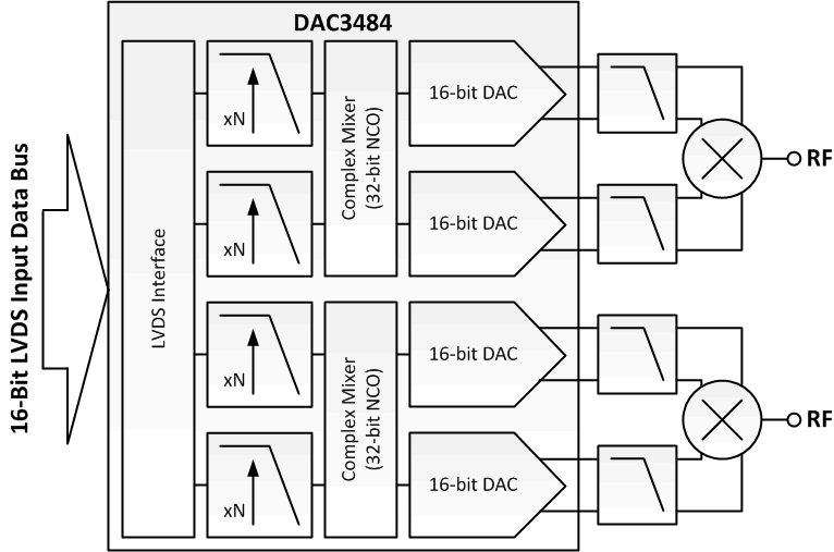
The DAC3484 is a very low power, high dynamic range, quad-channel, 16-bit digital-to-analog converter (DAC) with a sample rate as high as 1.25 GSPS.
The device includes features that simplify the design of complex transmit architectures: 2x to 16x digital interpolation filters with over 90dB of stop-band attenuation simplify the data interface and reconstruction filters. Independent complex mixers allow flexible carrier placement. A high-performance low jitter clock multiplier simplifies clocking of the device without significant impact on the dynamic range. The digital Quadrature Modulator Correction (QMC) enables complete IQ compensation for gain, offset, phase and group delay between channels in direct up-conversion applications.
Digital data is input to the device through a 16-bit LVDS data bus with on-chip termination. The device includes a FIFO, data pattern checker and parity test to ease the input interface. The interface also allows full synchronization of multiple devices.
The device is characterized for operation over the entire industrial temperature range of –40°C to 85°C and is available in a very-small 88-pin 9x9mm WQFN package or 196-ball 12x12mm NFBGA package.
Very low power, small size, superior crosstalk, high dynamic range and features of the DAC3484 are an ideal fit for systems with multiple transmit channels.
Device Information(1)
| PART NUMBER | PACKAGE | BODY SIZE (NOM) |
|---|---|---|
| DAC3484 | WQFN (88) | 9.00 mm x 9.00 mm |
| NFBGA (196) | 12.00 mm x 12.00 mm |
- For all available packages, see the orderable addendum at the end of the data sheet.
Simplified Schematic
