-
DRV401-Q1 Sensor Signal Conditioning Device for Closed-Loop Magnetic Current Sensor
- 1 Features
- 2 Applications
- 3 Description
- 4 Revision History
- 5 Pin Configuration and Functions
- 6 Specifications
-
7 Detailed Description
- 7.1 Overview
- 7.2 Functional Block Diagram
- 7.3
Feature Description
- 7.3.1 Magnetic Probe (Sensor) Interface
- 7.3.2 PWM Processing
- 7.3.3 Compensation Driver
- 7.3.4 External Compensation Coil Driver
- 7.3.5 Shunt Sense Amplifier
- 7.3.6 Over-Range Comparator
- 7.3.7 Voltage Reference
- 7.3.8 Demagnetization
- 7.3.9 Power-On and Brownout
- 7.3.10 Error Conditions
- 7.3.11 Protection Recommendations
- 7.4 Device Functional Modes
- 8 Application and Implementation
- 9 Power Supply Recommendations
- 10Layout
- 11Device and Documentation Support
- 12Mechanical, Packaging, and Orderable Information
- IMPORTANT NOTICE
Package Options
Mechanical Data (Package|Pins)
- RGW|20
Thermal pad, mechanical data (Package|Pins)
- RGW|20
Orderable Information
DRV401-Q1 Sensor Signal Conditioning Device for Closed-Loop Magnetic Current Sensor
1 Features
- Qualified for Automotive Applications
- AEC-Q100 Qualified With the Following Results:
- Device Temperature Grade 1: –40°C to +125°C Ambient Operating Temperature Range
- Device HBM ESD Classification Level 1C
- Device CDM ESD Classification Level C6
- Single-Supply: 5-V
- Power Output: H-Bridge
- Designed for Driving Inductive Loads
- Excellent DC Precision
- Wide System Bandwidth
- High-Resolution, Low-Temperature Drift
- Built-In Degauss System
- Extensive Fault Detection
- External High-Power Driver Option
- Compact Footprint
2 Applications
- Automotive
- Motor Control in Automotive Applications
- Flux Gate Current Sensing
- Generator and Alternator Monitoring and Control
- Frequency and Voltage Inverters
- Motor Drive Controllers
- System Power Consumption
- Photovoltaic Systems
3 Description
The DRV401-Q1 device is fully qualified for automotive applications and is suitable for motor control drive and battery monitoring systems.
When used with a magnetic sensor, the DRV401-Q1 monitors ac and dc currents to high accuracy.
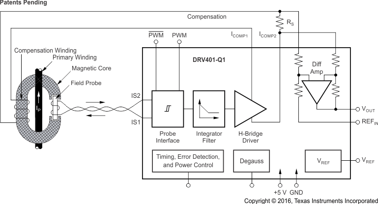
Provided functions include: probe excitation, signal conditioning of the probe signal, signal loop amplifier, an H-bridge driver for the compensation coil, and an analog signal output stage that provides an output voltage proportional to the primary current. It offers overload and fault detection, as well as transient noise suppression.
The DRV401-Q1 device directly drives the compensation coil or connects to external power drivers. Therefore, the DRV401-Q1 combines with sensors to measure small to large currents.
To maintain the highest accuracy, the DRV401-Q1 demagnetizes (degausses) the sensor at power-up and on demand.
Device Information(1)
| PART NUMBER | PACKAGE | BODY SIZE (NOM) |
|---|---|---|
| DRV401-Q1 | VQFN-20 | 5.00 mm × 5.00 mm |
- For all available packages, see the orderable addendum at the end of the data sheet.
Closed-Loop Magnetic Sensing

4 Revision History
| DATE | REVISION | NOTES |
|---|---|---|
| December 2016 | * | Initial release. |
5 Pin Configuration and Functions

Pin Functions
| PIN | I/O | DESCRIPTION | |
|---|---|---|---|
| NAME | NO. | ||
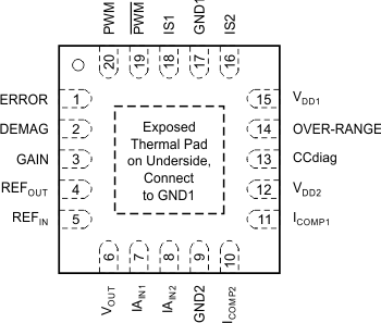
| CCdiag | 13 | I | Control input for wire-break detection: high = enable |
| DEMAG | 2 | I | Control input; See the Demagnetization section. |
| ERROR | 1 | O | Error flag: open-drain output. See the Error Conditions section. |
| GAIN | 3 | I | Control input for open-loop gain: low = normal, high = −8 dB |
| GND1 | 17 | — | Ground connection |
| GND2 | 9 | — | Ground connection. Connect to GND1. |
| IAIN1 | 8 | I | Inverting input of differential amplifier |
| IAIN2 | 7 | I | Noninverting input of differential amplifier |
| ICOMP1 | 11 | O | Output 1 of compensation coil driver |
| ICOMP2 | 10 | O | Output 2 of compensation coil driver |
| IS1 | 18 | I/O | Probe connection 1 |
| IS2 | 16 | I/O | Probe connection 2 |
| OVER-RANGE | 14 | O | Open-drain output for overrange indication: low = overrange |
| PWM | 19 | O | PWM output from probe circuit (inverted) |
| PWM | 20 | O | PWM output from probe circuit |
| REFOUT | 4 | O | Output for internal 2.5-V reference voltage |
| REFIN | 5 | I | Input for zero reference to differential amplifier |
| Thermal pad | — | — | Exposed thermal pad. Connect to GND1. |
| VDD1 | 15 | — | Supply voltage |
| VDD2 | 12 | — | Supply voltage. Connect to VDD1. |
| VOUT | 6 | O | Output for differential amplifier |