-
DRV425 Fluxgate Magnetic-Field Sensor
- 1 Features
- 2 Applications
- 3 Description
- 4 Revision History
- 5 Pin Configuration and Functions
- 6 Specifications
- 7 Detailed Description
- 8 Application and Implementation
- 9 Power-Supply Recommendations
- 10Layout
- 11Device and Documentation Support
- 12Mechanical, Packaging, and Orderable Information
- IMPORTANT NOTICE
Package Options
Mechanical Data (Package|Pins)
- RTJ|20
Thermal pad, mechanical data (Package|Pins)
- RTJ|20
Orderable Information
DRV425 Fluxgate Magnetic-Field Sensor
1 Features
- High-Precision, Integrated Fluxgate Sensor:
- Offset: ±8 µT (Max)
- Offset Drift: ±5 nT/°C (Typ)
- Gain Error: 0.04% (Typ)
- Gain Drift: ±7 ppm/°C (Typ)
- Linearity: ±0.1%
- Noise: 1.5 nT/√Hz (Typ)
- Sensor Range: ±2 mT (Max)
- Range and Gain Adjustable with External Resistor
- Selectable Bandwidth: 47 kHz or 32 kHz
- Precision Reference:
- Accuracy: 2% (max), Drift: 50 ppm/°C (max)
- Pin-Selectable Voltage: 2.5 V or 1.65 V
- Selectable Ratiometric Mode: VDD / 2
- Diagnostic Features: Overrange and Error Flags
- Supply Voltage Range: 3.0 V to 5.5 V
2 Applications
3 Description
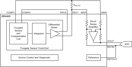
The DRV425 is designed for single-axis magnetic field-sensing applications and enables electrically-isolated, high-sensitivity, and precise dc- and ac-field measurements. The device provides the unique and proprietary, integrated fluxgate sensor (IFG) with an internal compensation coil to support a high-accuracy sensing range of ±2 mT with a measurement bandwidth of up to 47 kHz. The low offset, offset drift, and noise of the sensor, combined with the precise gain, low gain drift, and very low nonlinearity provided by the internal compensation coil, result in unrivaled magnetic field measurement precision. The output of the DRV425 is an analog signal proportional to the sensed magnetic field.
The DRV425 offers a complete set of features, including an internal difference amplifier, on-chip precision reference, and diagnostic functions to minimize component count and system-level cost.
The DRV425 is available in a thermally-enhanced, non-magnetic, thin WQFN package with a PowerPAD™ for optimized heat dissipation, and is specified for operation over the extended industrial temperature range of –40°C to +125°C.
Device Information (1)
| PART NUMBER | PACKAGE | BODY SIZE (NOM) |
|---|---|---|
| DRV425 | WQFN (20) | 4.00 mm × 4.00 mm |
- For all available packages, see the orderable addendum at the end of the data sheet.
Simplified Schematic

5 Pin Configuration and Functions

Pin Functions
| PIN | I/O | DESCRIPTION | |
|---|---|---|---|
| NAME | NO. | ||
| AINN | 14 | I | Inverting input of the shunt-sense amplifier |
| AINP | 13 | I | Noninverting input of the shunt-sense amplifier |
| BSEL | 1 | I | Filter bandwidth select input |
| COMP1 | 16 | I | Internal compensation coil input 1 |
| COMP2 | 17 | I | Internal compensation coil input 2 |
| DRV1 | 12 | O | Compensation coil driver output 1 |
| DRV2 | 11 | O | Compensation coil driver output 2 |
| ERROR | 19 | O | Error flag: open-drain, active-low output |
| GND | 7, 10, 18, 20 | — | Ground reference |
| OR | 15 | O | Shunt-sense amplifier overrange indicator: open-drain, active-low output |
| PowerPAD | — | Connect the thermal pad to GND | |
| REFIN | 5 | I | Common-mode reference input for the shunt-sense amplifier |
| REFOUT | 4 | O | Voltage reference output |
| RSEL0 | 3 | I | Voltage reference mode selection input 0 |
| RSEL1 | 2 | I | Voltage reference mode selection input 1 |
| VDD | 8, 9 | — | Supply voltage, 3.0 V to 5.5 V. Decouple both pins using 1-µF ceramic capacitors placed as close as possible to the device. See the Power-Supply Decoupling and Layout sections for further details. |
| VOUT | 6 | O | Shunt-sense amplifier output |