-
DRV8303 Three-Phase Gate Driver With Dual-Current Shunt Amplifiers
- 1 Features
- 2 Applications
- 3 Description
- 4 Revision History
- 5 Pin Configuration and Functions
-
6 Specifications
- 6.1 Absolute Maximum Ratings
- 6.2 ESD Ratings
- 6.3 Recommended Operating Conditions
- 6.4 Thermal Information
- 6.5 Electrical Characteristics
- 6.6 Current Shunt Amplifier Characteristics
- 6.7 SPI Characteristics (Slave Mode Only)
- 6.8 Gate Timing and Protection Switching Characteristics
- 6.9 Typical Characteristics
- 7 Detailed Description
- 8 Application and Implementation
- 9 Power Supply Recommendations
- 10Layout
- 11Device and Documentation Support
- 12Mechanical, Packaging, and Orderable Information
- IMPORTANT NOTICE
Package Options
Mechanical Data (Package|Pins)
- DCA|48
Thermal pad, mechanical data (Package|Pins)
- DCA|48
Orderable Information
DRV8303 Three-Phase Gate Driver With Dual-Current Shunt Amplifiers
1 Features
- 6-V to 60-V Operating Supply Voltage Range
- 1.7-A Source and 2.3-A Sink Gate Drive Current Capability
- Slew Rate Control for EMI Reduction
- Bootstrap Gate Driver With 100% Duty Cycle Support
- 6 or 3 PWM Input Modes
- Dual Integrated Current-Shunt Amplifiers With Adjustable Gain and Offset
- 3.3-V and 5-V Interface Support
- Serial Peripheral Interface (SPI)
- Protection Features:
- Programmable Dead Time Control (DTC)
- Programmable Overcurrent Protection (OCP)
- PVDD and GVDD Undervoltage Lockout (UVLO)
- GVDD Overvoltage Lockout (OVLO)
- Overtemperature Warning/Shutdown (OTW/OTS)
- Reported through nFAULT, nOCTW, and SPI Registers
2 Applications
- 3-Phase BLDC and PMSM Motors
- CPAP and Pump
- E-Bikes
- Power Tools
- Robotics and RC Toys
- Industrial Automation
3 Description
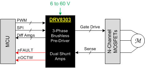
The DRV8303 is a gate driver IC for three-phase motor-drive applications. The device provides three half bridge drivers, each capable of driving two N-channel MOSFETs. The device supports up to 1.7-A source and 2.3-A peak current capability. The DRV8303 can operate off of a single power supply with a wide range from 6-V to 60-V. It uses a bootstrap gate-driver architecture with trickle charge circuitry to support 100% duty cycle. The DRV8303 uses automatic hand shaking when the high-side or low-side MOSFET is switching to prevent current shoot through. Integrated VDS sensing of the high-side and low-side MOSFETs is used to protect the external power stage against overcurrent conditions.
The DRV8303 includes two current-shunt amplifiers for accurate current measurement. The amplifiers support bi-directional current sensing and provide and adjustable output offset up to 3 V.
The serial peripheral interface (SPI) provides detailed fault reporting and flexible parameter settings such as gain options for the current-shunt amplifiers and slew-rate control of the gate drivers.
Device Information(1)
| PART NUMBER | PACKAGE | BODY SIZE (NOM) |
|---|---|---|
| DRV8303 | TSSOP (48) | 12.50 mm × 6.10 mm |
- For all available packages, see the orderable addendum at the end of the data sheet.
4 Revision History
Changes from B Revision (November 2015) to C Revision
- Added the maximum voltage difference and maximum voltage parameters for the BST_X, GH_X, SL_X, and SH_X pins in the Absolute Maximum Ratings tableGo
- Added the Documentation support and Receiving Notification of Documentation Updates sections Go
Changes from A Revision (October 2013) to B Revision
- Added ESD Ratings table, Feature Description section, Device Functional Modes, Application and Implementation section, Power Supply Recommendations section, Layout section, Device and Documentation Support section, and Mechanical, Packaging, and Orderable Information section Go
- Updated titleGo
- VPVDD absolute max voltage rating reduced from 70 V to 65 V Go
- Clarification made on how the OCP status bits report in Overcurrent Protection (OCP) and Reporting Go
- Update to PVDD undervoltage protection in Undervoltage Protection (UVLO) describing specific transient brownout issue.Go
- Update to EN_GATE pin functional description in EN_GATE clarifying proper EN_GATE reset pulse lengths. Go
- Added gate driver power-up sequencing errata Go
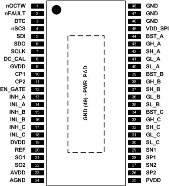
5 Pin Configuration and Functions

Pin Functions
| PIN | I/O | DESCRIPTION | |
|---|---|---|---|
| NO. | NAME | ||
| 1 | nOCTW | O | Overcurrent and overtemperature warning indicator. This output is open drain with external pullup resistor required. Programmable output mode through SPI registers. |
| 2 | nFAULT | O | Fault report indicator. This output is open drain with external pullup resistor required. |
| 3 | DTC | I | Dead-time adjustment with external resistor to GND |
| 4 | nSCS | I | SPI chip select |
| 5 | SDI | I | SPI input |
| 6 | SDO | O | SPI output |
| 7 | SCLK | I | SPI clock signal |
| 8 | DC_CAL | I | When DC_CAL is high, device shorts inputs of shunt amplifiers and disconnects loads. DC offset calibration can be done through external microcontroller. |
| 9 | GVDD | P | Internal gate driver voltage regulator. GVDD cap should connect to GND |
| 10 | CP1 | P | Charge pump pin 1, ceramic cap should be used between CP1 and CP2 |
| 11 | CP2 | P | Charge pump pin 2, ceramic cap should be used between CP1 and CP2 |
| 12 | EN_GATE | I | Enable gate driver and current shunt amplifiers. |
| 13 | INH_A | I | PWM Input signal (high side), half-bridge A |
| 14 | INL_A | I | PWM Input signal (low side), half-bridge A |
| 15 | INH_B | I | PWM Input signal (high side), half-bridge B |
| 16 | INL_B | I | PWM Input signal (low side), half-bridge B |
| 17 | INH_C | I | PWM Input signal (high side), half-bridge C |
| 18 | INL_C | I | PWM Input signal (low side), half-bridge C |
| 19 | DVDD | P | Internal 3.3-V supply voltage. DVDD cap should connect to AGND. This is an output, but not specified to drive external circuitry. |
| 20 | REF | I | Reference voltage to set output of shunt amplifiers with a bias voltage which equals to half of the voltage set on this pin. Connect to ADC reference in microcontroller. |
| 21 | SO1 | O | Output of current amplifier 1 |
| 22 | SO2 | O | Output of current amplifier 2 |
| 23 | AVDD | P | Internal 6-V supply voltage, AVDD capacitor should always be installed and connected to AGND. This is an output, but not specified to drive external circuitry. |
| 24 | AGND | P | Analog ground pin |
| 25 | PVDD | P | Power supply pin for gate driver, current shunt amplifier, and SPI communication. PVDD cap should connect to GND |
| 26 | SP2 | I | Input of current amplifier 2 (connecting to positive input of amplifier). Recommend to connect to ground side of the sense resistor for the best common mode rejection. |
| 27 | SN2 | I | Input of current amplifier 2 (connecting to negative input of amplifier). |
| 28 | SP1 | I | Input of current amplifier 1 (connecting to positive input of amplifier). Recommend to connect to ground side of the sense resistor for the best common mode rejection. |
| 29 | SN1 | I | Input of current amplifier 1 (connecting to negative input of amplifier). |
| 30 | SL_C | I | Low-Side MOSFET source connection, half-bridge C. Low-side VDS measured between this pin and SH_C. |
| 31 | GL_C | O | Gate drive output for Low-Side MOSFET, half-bridge C |
| 32 | SH_C | I | High-Side MOSFET source connection, half-bridge C. High-side VDS measured between this pin and PVDD. |
| 33 | GH_C | O | Gate drive output for High-Side MOSFET, half-bridge C |
| 34 | BST_C | P | Bootstrap capacitor pin for half-bridge C |
| 35 | SL_B | I | Low-Side MOSFET source connection, half-bridge B. Low-side VDS measured between this pin and SH_B. |
| 36 | GL_B | O | Gate drive output for Low-Side MOSFET, half-bridge B |
| 37 | SH_B | I | High-Side MOSFET source connection, half-bridge B. High-side VDS measured between this pin and PVDD. |
| 38 | GH_B | O | Gate drive output for High-Side MOSFET, half-bridge B |
| 39 | BST_B | P | Bootstrap cap pin for half-bridge B |
| 40 | SL_A | I | Low-Side MOSFET source connection, half-bridge A. Low-side VDS measured between this pin and SH_A. |
| 41 | GL_A | O | Gate drive output for Low-Side MOSFET, half-bridge A |
| 42 | SH_A | I | High-Side MOSFET source connection, half-bridge A. High-side VDS measured between this pin and PVDD. |
| 43 | GH_A | O | Gate drive output for High-Side MOSFET, half-bridge A |
| 44 | BST_A | P | Bootstrap capacitor pin for half-bridge A |
| 45 | VDD_SPI | I | SPI supply pin to support 3.3V or 5V logic. Connect to either 3.3V or 5V. |
| 469 | GND | O | GND pin. The exposed power pad must be electrically connected to ground plane through soldering to PCB for proper operation and connected to bottom side of PCB through vias for better thermal spreading. |
| 47 | |||
| 48 | |||
| 49 | GND (PWR_PAD) |
||
