DATA SHEET
EMB1412 MOSFET Gate Driver
1 Features
- Compound CMOS and Bipolar Outputs Reduce Output Current Variation
- 7 A Sink/3 A Source Current
- Fast Propagation Times (25 ns Typical)
- Fast Rise and Fall Times (14 ns/12 ns Rise/Fall with 2 nF Load)
- Inverting and Non-Inverting Inputs Provide Either Configuration with a Single Device
- Supply Rail Under-Voltage Lockout Protection
- Dedicated Input Ground (IN_REF) for Split Supply or Single Supply Operation
- Thermally Enhanced 8-Pin VSSOP Package
- Output Swings from VCC to VEE Which can be Negative Relative to Input Ground
2 Applications
- Li-Ion Battery Management Systems
- Hybrid and Electric Vehicles
- Grid Storage
- 48 V Systems Supply
- UPS
3 Description
The EMB1412 MOSFET gate driver provides high peak gate drive current in 8-lead exposed-pad VSSOP package, with improved power dissipation required for high frequency operation. The compound output driver stage includes MOS and bipolar transistors operating in parallel that together sink more than 7-A peak from capacitive loads. Combining the unique characteristics of MOS and bipolar devices reduces drive current variation with voltage and temperature. Under-voltage lockout protection is provided to prevent damage to the MOSFET due to insufficient gate turn-on voltage. The EMB1412 provides both inverting and non-inverting inputs to satisfy requirements for inverting and non-inverting gate drive with a single device type.
Device Information(1)
| PART NUMBER | PACKAGE | BODY SIZE (NOM) |
|---|---|---|
| EMB1412 | HVSSOP (8) | 3.00 mm x 3.00 mm |
- For all available packages, see the orderable addendum at the end of the datasheet.
5 Pin Configuration and Functions
VSSOP (DGN)
8 Pins
Top View
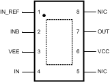
Pin Functions
| PIN | NAME | DESCRIPTION | APPLICATION INFORMATION |
|---|---|---|---|
| 1 | IN_REF | Ground reference for control inputs | Connect to power ground (VEE) for standard positive only output voltage swing. Connect to system logic ground when VEE is connected to a negative gate drive supply. |
| 2 | INB | Inverting input pin | TTL compatible thresholds. Connect to IN_REF when not used. |
| 3 | VEE | Power ground for driver outputs | Connect to either power ground or a negative gate drive supply for positive or negative voltage swing. |
| 4 | IN | Non-inverting input pin | TTL compatible thresholds. Pull up to VCC when not used. |
| 5, 8 | N/C | Not internally connected | |
| 6 | VCC | Positive Supply voltage input | Locally decouple to VEE. The decoupling capacitor should be located close to the chip. |
| 7 | OUT | Gate drive output | Capable of sourcing 3 A and sinking 7 A. Voltage swing of this output is from VEE to VCC. |
| - - - | Exposed Pad | Exposed Pad, underside of package | Internally bonded to the die substrate. Connect to VEE ground pin for low thermal impedance. |
6 Specifications
6.1 Absolute Maximum Ratings(1)
| MIN | MAX | UNIT | |
|---|---|---|---|
| VCC to VEE | −0.3 | 15 | V |
| VCC to IN_REF | −0.3 | 15 | V |
| IN/INB to IN_REF | −0.3 | 15 | V |
| IN_REF to VEE | −0.3 | 5 | V |
| Maximum junction temperature | 150 | °C |
(1) Stresses beyond those listed under Absolute Maximum Ratings may cause permanent damage to the device. These are stress ratings only, which do not imply functional operation of the device at these or any other conditions beyond those indicated under Recommended Operating Conditions. Exposure to absolute-maximum-rated conditions for extended periods may affect device reliability.
6.2 Handling Ratings
| MIN | MAX | UNIT | |||
|---|---|---|---|---|---|
| Tstg | Storage temperature range | –55 | 150 | °C | |
| V(ESD) | Electrostatic discharge | Human body model (HBM), per ANSI/ESDA/JEDEC JS-001, all pins(1) | 2 | kV | |
(1) JEDEC document JEP155 states that 500-V HBM allows safe manufacturing with a standard ESD control process.
6.3 Recommended Operating Conditions
over operating free-air temperature range (unless otherwise noted)| MIN | NOM | MAX | UNIT | ||
|---|---|---|---|---|---|
| Operating Junction Temperature | −40 | 125 | °C | ||
6.4 Thermal Information
| THERMAL METRIC(1) | EMB1412 | UNIT | |
|---|---|---|---|
| VSSOP (DGN) | |||
| 8 PINS | |||
| RθJA | Junction-to-ambient thermal resistance | 60(2) | °C/W |
| RθJCbot | Junction-to-case (bottom) thermal resistance | 4.7 | |
(1) For more information about traditional and new thermal metrics, see the IC Package Thermal Metrics application report, SPRA953.
(2) The primary goal of the thermal management is to maintain the integrated circuit (IC) junction temperature (TJ) below a specified limit to ensure reliable long term operation. The maximum TJ of IC components should be estimated in worst case operating conditions. The junction temperature can be calculated based on the power dissipated on the IC and the junction to ambient thermal resistance RθJA for the IC package in the application board and environment. The RθJA is not a given constant for the package and depends on the PCB design and the operating environment.
6.5 Electrical Characteristics
TJ = −40°C to 125°C, VCC = 12 V, INB = IN_REF = VEE = 0 V, No Load on output, unless otherwise specified.| PARAMETER | TEST CONDITIONS | MIN | TYP | MAX | UNIT | |
|---|---|---|---|---|---|---|
| SUPPLY | ||||||
| VCC | VCC Operating Range | VCC – IN_REF and VCC - VEE | 3.5 | 14 | V | |
| UVLO | VCC Under-voltage Lockout (rising) | VCC – IN_REF | 2.4 | 3.0 | 3.5 | V |
| VCCH | VCC Under-voltage Hysteresis | 230 | mV | |||
| ICC | VCC Supply Current | 1.0 | 2.0 | mA | ||
| CONTROL INPUTS | ||||||
| VIH | Logic High | 2.3 | V | |||
| VIL | Logic Low | 0.8 | V | |||
| VthH | High Threshold | 1.3 | 1.75 | 2.3 | V | |
| VthL | Low Threshold | 0.8 | 1.35 | 2.0 | V | |
| HYS | Input Hysteresis | 400 | mV | |||
| IIL | Input Current Low | IN = INB = 0 V | -1 | 0.1 | 1 | µA |
| IIH | Input Current High | IN = INB = VCC | -1 | 0.1 | 1 | µA |
| OUTPUT DRIVER | ||||||
| ROH | Output Resistance High | IOUT = -10 mA(1) | 30 | 50 | Ω | |
| ROL | Output Resistance Low | IOUT = 10 mA(1) | 1.4 | 2.5 | Ω | |
| ISOURCE | Peak Source Current | OUT = VCC/2, 200 ns pulsed current | 3 | A | ||
| ISINK | Peak Sink Current | OUT = VCC/2, 200 ns pulsed current | 7 | A | ||
| SWITCHING CHARACTERISTICS | ||||||
| td1 | Propagation Delay Time Low to High, IN/ INB rising ( IN to OUT) |
CLOAD = 2 nF | 25 | 40 | ns | |
| td2 | Propagation Delay Time High to Low, IN / INB falling (IN to OUT) |
CLOAD = 2 nF | 25 | 40 | ns | |
| tr | Rise time | CLOAD = 2 nF | 14 | ns | ||
| tf | Fall time | CLOAD = 2 nF | 12 | ns | ||
| LATCHUP PROTECTION | ||||||
| AEC –Q100, METHOD 004 | TJ = 150°C | 500 | mA | |||
| THERMAL RESISTANCE | ||||||
| RθJA | Junction to Ambient, 0 LFPM Air Flow |
VSSOP Package | 60 | °C/W | ||
| RθJC | Junction to Case | VSSOP Package | 4.7 | °C/W | ||
(1) The output resistance specification applies to the MOS device only. The total output current capability is the sum of the MOS and Bipolar devices.
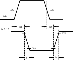 Figure 1. (A) Inverting
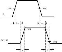 Figure 2. (B) Non-Inverting