-
ISO308x Isolated 5-V Full- and Half-Duplex RS-485 Transceivers
- 1
- 1 Features
- 2 Applications
- 3 Description
- 4 Revision History
- 5 Pin Configuration and Functions
-
6 Specifications
- 6.1 Absolute Maximum Ratings
- 6.2 ESD Ratings
- 6.3 Recommended Operating Conditions
- 6.4 Thermal Information
- 6.5 Insulation Specifications
- 6.6 Safety-Related Certifications
- 6.7 Safety Limiting Values
- 6.8 Electrical Characteristics: Driver
- 6.9 Electrical Characteristics: Receiver
- 6.10 Supply Current
- 6.11 Switching Characteristics: Driver
- 6.12 Switching Characteristics: Receiver
- 6.13 Insulation Characteristics Curves
- 6.14 Typical Characteristics
- 7 Parameter Measurement Information
- 8 Detailed Description
- 9 Application and Implementation
- 10Power Supply Recommendations
- 11Layout
- 12Device and Documentation Support
- 13Mechanical, Packaging, and Orderable Information
- IMPORTANT NOTICE
Package Options
Refer to the PDF data sheet for device specific package drawings
Mechanical Data (Package|Pins)
- DW|16
Thermal pad, mechanical data (Package|Pins)
Orderable Information
ISO308x Isolated 5-V Full- and Half-Duplex RS-485 Transceivers
1 Features
- Meets or exceeds TIA/EIA RS-485 requirements
- Signaling rates up to 20 Mbps
- 1/8 unit load – up to 256 nodes on a bus
- Thermal shutdown protection
- Low bus capacitance – 16 pF (typical)
- 50 kV/μs typical transient immunity
- Fail-safe receiver for bus open, short, idle
- 3.3-V inputs are 5-V tolerant
- Bus-pin ESD protection
- 12-kV HBM between bus pins and GND2
- 6-kV HBM between bus pins and GND1
- Safety-related certifications:
- 4000-VPK basic insulation, 560 VPK VIORM per DIN EN IEC 60747-17 (VDE 0884-17)
- 2500 VRMS isolation per UL 1577
- 4000 VPK isolation per CSA 62368-1
2 Applications
- Security systems
- Chemical production
- Factory automation
- Motor and motion control
- HVAC and building automation networks
- Networked security stations
3 Description
The ISO3080 and ISO3086 devices are isolated full-duplex differential line drivers and receivers while the ISO3082 and ISO3088 devices are isolated half-duplex differential line transceivers for TIA/EIA 485/422 applications.
These devices are ideal for long transmission lines because the ground loop is broken to allow for a much larger common-mode voltage range. The symmetrical isolation barrier of the device is tested to provide 2500 VRMS of isolation for 60 s per UL 1577 between the bus-line transceiver and the logic-level interface.
Any cabled I/O can be subjected to electrical noise transients from various sources. These noise transients can cause damage to the transceiver or nearby sensitive circuitry if they are of sufficient magnitude and duration. These isolated devices can significantly increase protection and reduce the risk of damage to expensive control circuits.
The ISO3080, ISO3082, ISO3086, and ISO3088 device are qualified for use from –40°C to +85°C.
| PART NUMBER | PACKAGE | BODY SIZE (NOM) |
|---|---|---|
| ISO3080 | SOIC (16) | 10.30 mm × 7.50 mm |
| ISO3082 | ||
| ISO3086 | ||
| ISO3088 |
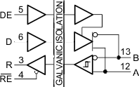
 ISO3080, IOS3086 Function
Diagram
 ISO3082, IOS3088 Function
Diagram
ISO3082, IOS3088 Function
Diagram4 Revision History
Changes from Revision I (April 2017) to Revision J (August 2023)
- Updated the numbering format for tables, figures, and cross-references throughout the documentGo
- Updated Thermal Characteristics, Safety Limiting Values, and Thermal Derating Curves to provide more accurate system-level thermal calculationsGo
- Updated electrical and switching characteristics to match device performanceGo
Changes from Revision H (December 2015) to Revision I (April 2017)
Changes from Revision G (July 2015) to Revision H (Devember 2015)
- Moved the last list item " Routing the high-speed traces..." to the second list items in Layout Guidelines sectionGo
Changes from Revision F (May 2015) to Revision G (July 2015)
- Changed the Layout Guidelines section Go
Changes from Revision E (September 2011) to Revision F (May 2015)
- Added ESD Rating table, Thermal Information table, Feature Description section, Device Functional Modes, Application and Implementation section, Power Supply Recommendations section, Layout section, Device and Documentation Support section, and Mechanical, Packaging, and Orderable Information sectionGo
- Changed Features list item From: IEC 60747-5-2 (VDE 0884, Rev. 2) To: DIN V VDE V 0884-10 (VDE V 0884-10): 2006-12Go
- VDE standard changed to DIN V VDE V 0884-10 (VDE V 0884-10):2006-12Go
Changes from Revision D (January 2011) to Revision E (September 2011)
- Changed Features list item From: 16 kV HBM To: 12 kV HBMGo
Changes from Revision C (October 2009) to Revision D (January 2011)
- Changed graph for " DW-16 θJC Thermal Derating Curve per IEC 60747-5-2 " , Thermal Derating Curve Go
- Added the ISO3086 Recommended Minimum Differential Input Voltage vs Signaling Rate graphGo
- Added note to bottom of first page of the Parameter Measurement Information Go
- Added Footnotes to the Driver Function Table and Receiver Function Table Go
Changes from Revision A (June 2008) to Revision B (December 2008)
- Changed Features bullet From: 4000-VPEAK Isolation, To: 4000-VPEAK Isolation,, 560-VPEAK VIORM Go
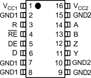
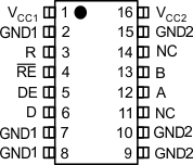
5 Pin Configuration and Functions
 Figure 5-1 ISO3080 and ISO3086 DW Package16-Pin SOICTop View
 Figure 5-2 ISO3082 and ISO3088 DW Package16-Pin SOICTop View
| PIN | I/O | DESCRIPTION | ||
|---|---|---|---|---|
| NAME | ISO3080, ISO3086 |
ISO3082, ISO3088 |
||
| A | 14 | — | I | Receiver noninverting input on the bus-side |
| — | 12 | I/O | Transceiver noninverting Input or output (I/O) on the bus-side | |
| B | 13 | — | I | Receiver inverting Input on the bus-side |
| — | 13 | I/O | Transceiver inverting input or output (I/O) on the bus-side | |
| D | 6 | 6 | I | Driver input |
| DE | 5 | 5 | I | Enables (when high) or disables (when low or open) driver output of ISO308x |
| GND1 | 2 | 2 | — | Ground connection for VCC1 |
| 7 | 7 | |||
| 8 | 8 | |||
| GND2 | 9 | 9 | — | Ground connection for VCC2 |
| 10 | 10 | |||
| 15 | 15 | |||
| NC | — | 11 | — | No connect |
| 14 | ||||
| R | 3 | 3 | O | Receiver output |
| RE | 4 | 4 | I | Disables (when high or open) or enables (when low) receiver output of ISO308x |
| VCC1 | 1 | 1 | — | Power supply, VCC1 |
| VCC2 | 16 | 16 | — | Power supply, VCC2 |
| Y | 11 | — | O | Driver noninverting output |
| Z | 12 | — | O | Driver inverting output |
6 Specifications
6.1 Absolute Maximum Ratings
| MIN | MAX | UNIT | ||
|---|---|---|---|---|
| VCC(2) | Supply voltage, VCC1, VCC2 | -0.3 | 6 | V |
| VO | Voltage at any bus I/O terminal | -9 | 14 | V |
| VIT | Voltage input, transient pulse, A, B, Y, and Z (through 100Ω, see Figure 21) | -50 | 50 | V |
| VI | Voltage input at any D, DE or RE terminal | -0.5 | 6 | V |
| IO | Receiver output current | -10 | 10 | mA |
| TJ | Junction temperature | 150 | ℃ | |
| TSTG | Storage temperature | -65 | 150 | ℃ |