-
LM35 Precision Centigrade Temperature Sensors
- 1 Features
- 2 Applications
- 3 Description
- 4 Revision History
- 5 Pin Configuration and Functions
-
6 Specifications
- 6.1 Absolute Maximum Ratings
- 6.2 ESD Ratings
- 6.3 Recommended Operating Conditions
- 6.4 Thermal Information
- 6.5 Electrical Characteristics: LM35A, LM35CA Limits
- 6.6 Electrical Characteristics: LM35A, LM35CA
- 6.7 Electrical Characteristics: LM35, LM35C, LM35D Limits
- 6.8 Electrical Characteristics: LM35, LM35C, LM35D
- 6.9 Typical Characteristics
- 7 Detailed Description
- 8 Application and Implementation
- 9 Power Supply Recommendations
- 10Layout
- 11Device and Documentation Support
- 12Mechanical, Packaging, and Orderable Information
- IMPORTANT NOTICE
Package Options
Refer to the PDF data sheet for device specific package drawings
Mechanical Data (Package|Pins)
- D|8
- NDV|3
- LP|3
- NEB|3
Thermal pad, mechanical data (Package|Pins)
Orderable Information
LM35 Precision Centigrade Temperature Sensors
1 Features
- Calibrated Directly in Celsius (Centigrade)
- Linear + 10-mV/°C Scale Factor
- 0.5°C Ensured Accuracy (at 25°C)
- Rated for Full −55°C to 150°C Range
- Suitable for Remote Applications
- Low-Cost Due to Wafer-Level Trimming
- Operates From 4 V to 30 V
- Less Than 60-μA Current Drain
- Low Self-Heating, 0.08°C in Still Air
- Non-Linearity Only ±¼°C Typical
- Low-Impedance Output, 0.1 Ω for 1-mA Load
2 Applications
- Power Supplies
- Battery Management
- HVAC
- Appliances
3 Description
The LM35 series are precision integrated-circuit temperature devices with an output voltage linearly-proportional to the Centigrade temperature. The LM35 device has an advantage over linear temperature sensors calibrated in Kelvin, as the user is not required to subtract a large constant voltage from the output to obtain convenient Centigrade scaling. The LM35 device does not require any external calibration or trimming to provide typical accuracies of ±¼°C at room temperature and ±¾°C over a full −55°C to 150°C temperature range. Lower cost is assured by trimming and calibration at the wafer level. The low-output impedance, linear output, and precise inherent calibration of the LM35 device makes interfacing to readout or control circuitry especially easy. The device is used with single power supplies, or with plus and minus supplies. As the LM35 device draws only 60 μA from the supply, it has very low self-heating of less than 0.1°C in still air. The LM35 device is rated to operate over a −55°C to 150°C temperature range, while the LM35C device is rated for a −40°C to 110°C range (−10° with improved accuracy). The LM35-series devices are available packaged in hermetic TO transistor packages, while the LM35C, LM35CA, and LM35D devices are available in the plastic TO-92 transistor package. The LM35D device is available in an 8-lead surface-mount small-outline package and a plastic TO-220 package.
Device Information(1)
| PART NUMBER | PACKAGE | BODY SIZE (NOM) |
|---|---|---|
| LM35 | TO-CAN (3) | 4.699 mm × 4.699 mm |
| TO-92 (3) | 4.30 mm × 4.30 mm | |
| SOIC (8) | 4.90 mm × 3.91 mm | |
| TO-220 (3) | 14.986 mm × 10.16 mm |
- For all available packages, see the orderable addendum at the end of the datasheet.
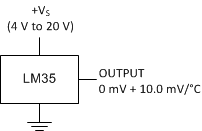
Basic Centigrade Temperature Sensor
(2°C to 150°C)
Full-Range Centigrade Temperature Sensor
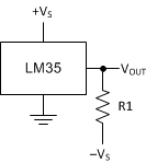
VOUT = 1500 mV at 150°C
VOUT = 250 mV at 25°C
VOUT = –550 mV at –55°C
4 Revision History
Changes from G Revision (August 2016) to H Revision
- Changed NDV Package (TO-CAN) pinout from bottom view back to top view; added textnote to pinoutGo
- Added pin numbers to the TO-CAN (TO46) pinoutGo
Changes from F Revision (January 2016) to G Revision
- Equation 1, changed From: 10 mV/°F To: 10mv/°C Go
- Power Supply Recommendations, changed From: "4-V to 5.5-V power supply" To: "4-V to 30-V power supply:Go
Changes from E Revision (January 2015) to F Revision
- Changed NDV Package (TO-CAN) pinout from Top View to Bottom ViewGo
Changes from D Revision (October 2013) to E Revision
- Added Pin Configuration and Functions section, ESD Ratings table, Feature Description section, Device Functional Modes, Application and Implementation section, Power Supply Recommendations section, Layout section, Device and Documentation Support section, and Mechanical, Packaging, and Orderable Information section Go
Changes from C Revision (July 2013) to D Revision
5 Pin Configuration and Functions


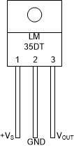
Pin Functions
| PIN | TYPE | DESCRIPTION | ||||
|---|---|---|---|---|---|---|
| NAME | TO46 | TO92 | TO220 | SO8 | ||
| VOUT | 2 | 2 | 3 | 1 | O | Temperature Sensor Analog Output |
| N.C. | — | — | — | 2 | — | No Connection |
| — | — | — | 3 | |||
| GND | 3 | 3 | 2 | 4 | GROUND | Device ground pin, connect to power supply negative terminal |
| N.C. | — | — | — | 5 | — | No Connection |
| — | — | — | 6 | |||
| — | — | — | 7 | |||
| +VS | 1 | 1 | 1 | 8 | POWER | Positive power supply pin |
6 Specifications
6.1 Absolute Maximum Ratings
over operating free-air temperature range (unless otherwise noted)(1)(2)| MIN | MAX | UNIT | |||
|---|---|---|---|---|---|
| Supply voltage | –0.2 | 35 | V | ||
| Output voltage | –1 | 6 | V | ||
| Output current | 10 | mA | |||
| Maximum Junction Temperature, TJmax | 150 | °C | |||
| Storage Temperature, Tstg | TO-CAN, TO-92 Package | –60 | 150 | °C | |
| TO-220, SOIC Package | –65 | 150 | |||
6.2 ESD Ratings
| VALUE | UNIT | |||
|---|---|---|---|---|
| V(ESD) | Electrostatic discharge | Human-body model (HBM), per ANSI/ESDA/JEDEC JS-001(1) | ±2500 | V |
6.3 Recommended Operating Conditions
over operating free-air temperature range (unless otherwise noted)| MIN | MAX | UNIT | ||
|---|---|---|---|---|
| Specified operating temperature: TMIN to TMAX | LM35, LM35A | –55 | 150 | °C |
| LM35C, LM35CA | –40 | 110 | ||
| LM35D | 0 | 100 | ||
| Supply Voltage (+VS) | 4 | 30 | V | |
6.4 Thermal Information
| THERMAL METRIC(1)(2) | LM35 | UNIT | ||||
|---|---|---|---|---|---|---|
| NDV | LP | D | NEB | |||
| 3 PINS | 8 PINS | 3 PINS | ||||
| RθJA | Junction-to-ambient thermal resistance | 400 | 180 | 220 | 90 | °C/W |
| RθJC(top) | Junction-to-case (top) thermal resistance | 24 | — | — | — | |
6.5 Electrical Characteristics: LM35A, LM35CA Limits
Unless otherwise noted, these specifications apply: −55°C ≤ TJ ≤ 150°C for the LM35 and LM35A; −40°C ≤ TJ ≤ 110°C for the LM35C and LM35CA; and 0°C ≤ TJ ≤ 100°C for the LM35D. VS = 5 Vdc and ILOAD = 50 μA, in the circuit of Full-Range Centigrade Temperature Sensor. These specifications also apply from 2°C to TMAX in the circuit of Figure 14.| PARAMETER | TEST CONDITIONS | LM35A | LM35CA | UNIT | ||||
|---|---|---|---|---|---|---|---|---|
| TYP | TESTED LIMIT(2) | DESIGN LIMIT(3) | TYP | TESTED LIMIT(2) | DESIGN LIMIT(3) | |||
| Accuracy(4) | TA = 25°C | ±0.2 | ±0.5 | ±0.2 | ±0.5 | °C | ||
| TA = –10°C | ±0.3 | ±0.3 | ±1 | |||||
| TA = TMAX | ±0.4 | ±1 | ±0.4 | ±1 | ||||
| TA = TMIN | ±0.4 | ±1 | ±0.4 | ±1.5 | ||||
| Nonlinearity(5) | TMIN ≤ TA ≤ TMAX, –40°C ≤ TJ ≤ 125°C |
±0.18 | ±0.35 | ±0.15 | ±0.3 | °C | ||
| Sensor gain (average slope) |
TMIN ≤ TA ≤ TMAX | 10 | 9.9 | 10 | 9.9 | mV/°C | ||
| –40°C ≤ TJ ≤ 125°C | 10 | 10.1 | 10 | 10.1 | ||||
| Load regulation(1)
0 ≤ IL ≤ 1 mA |
TA = 25°C | ±0.4 | ±1 | ±0.4 | ±1 | mV/mA | ||
| TMIN ≤ TA ≤ TMAX, –40°C ≤ TJ ≤ 125°C |
±0.5 | ±3 | ±0.5 | ±3 | ||||
| Line regulation(1) | TA = 25°C | ±0.01 | ±0.05 | ±0.01 | ±0.05 | mV/V | ||
| 4 V ≤ VS ≤ 30 V, –40°C ≤ TJ ≤ 125°C |
±0.02 | ±0.1 | ±0.02 | ±0.1 | ||||
| Quiescent current(6) | VS = 5 V, 25°C | 56 | 67 | 56 | 67 | µA | ||
| VS = 5 V, –40°C ≤ TJ ≤ 125°C | 105 | 131 | 91 | 114 | ||||
| VS = 30 V, 25°C | 56.2 | 68 | 56.2 | 68 | ||||
| VS = 30 V, –40°C ≤ TJ ≤ 125°C | 105.5 | 133 | 91.5 | 116 | ||||
| Change of quiescent current(1) | 4 V ≤ VS ≤ 30 V, 25°C | 0.2 | 1 | 0.2 | 1 | µA | ||
| 4 V ≤ VS ≤ 30 V, –40°C ≤ TJ ≤ 125°C |
0.5 | 2 | 0.5 | 2 | ||||
| Temperature coefficient of quiescent current | –40°C ≤ TJ ≤ 125°C | 0.39 | 0.5 | 0.39 | 0.5 | µA/°C | ||
| Minimum temperature for rate accuracy | In circuit of Figure 14, IL = 0 | 1.5 | 2 | 1.5 | 2 | °C | ||
| Long term stability | TJ = TMAX, for 1000 hours | ±0.08 | ±0.08 | °C | ||||
6.6 Electrical Characteristics: LM35A, LM35CA
Unless otherwise noted, these specifications apply: −55°C ≤ TJ ≤ 150°C for the LM35 and LM35A; −40°C ≤ TJ ≤ 110°C for the LM35C and LM35CA; and 0°C ≤ TJ ≤ 100°C for the LM35D. VS = 5 Vdc and ILOAD = 50 μA, in the circuit of Full-Range Centigrade Temperature Sensor. These specifications also apply from 2°C to TMAX in the circuit of Figure 14.| PARAMETER | TEST CONDITIONS | LM35A | LM35CA | UNIT | |||||
|---|---|---|---|---|---|---|---|---|---|
| MIN | TYP | MAX | TYP | TYP | MAX | ||||
| Accuracy(4) | TA = 25°C | ±0.2 | ±0.2 | °C | |||||
| Tested Limit(2) | ±0.5 | ±0.5 | |||||||
| Design Limit(3) | |||||||||
| TA = –10°C | ±0.3 | ±0.3 | |||||||
| Tested Limit(2) | |||||||||
| Design Limit(3) | ±1 | ||||||||
| TA = TMAX | ±0.4 | ±0.4 | |||||||
| Tested Limit(2) | ±1 | ±1 | |||||||
| Design Limit(3) | |||||||||
| TA = TMIN | ±0.4 | ±0.4 | |||||||
| Tested Limit(2) | ±1 | ||||||||
| Design Limit(3) | ±1.5 | ||||||||
| Nonlinearity(5) | TMIN ≤ TA ≤ TMAX, –40°C ≤ TJ ≤ 125°C |
±0.18 | ±0.15 | °C | |||||
| Tested Limit(2) | |||||||||
| Design Limit(3) | ±0.35 | ±0.3 | |||||||
| Sensor gain (average slope) |
TMIN ≤ TA ≤ TMAX | 10 | 10 | mV/°C | |||||
| Tested Limit(2) | 9.9 | ||||||||
| Design Limit(3) | 9.9 | ||||||||
| –40°C ≤ TJ ≤ 125°C | 10 | 10 | |||||||
| Tested Limit(2) | 10.1 | ||||||||
| Design Limit(3) | 10.1 | ||||||||
| Load regulation(1)
0 ≤ IL ≤ 1 mA |
TA = 25°C | ±0.4 | ±0.4 | mV/mA | |||||
| Tested Limit(2) | ±1 | ±1 | |||||||
| Design Limit(3) | |||||||||
| TMIN ≤ TA ≤ TMAX, –40°C ≤ TJ ≤ 125°C |
±0.5 | ±0.5 | |||||||
| Tested Limit(2) | |||||||||
| Design Limit(3) | ±3 | ±3 | |||||||
| Line regulation(1) | TA = 25°C | ±0.01 | ±0.01 | mV/V | |||||
| Tested Limit(2) | ±0.05 | ±0.05 | |||||||
| Design Limit(3) | |||||||||
| 4 V ≤ VS ≤ 30 V, –40°C ≤ TJ ≤ 125°C |
±0.02 | ±0.02 | |||||||
| Tested Limit(2) | |||||||||
| Design Limit(3) | ±0.1 | ±0.1 | |||||||
| Quiescent current(6) | VS = 5 V, 25°C | 56 | 56 | µA | |||||
| Tested Limit(2) | 67 | 67 | |||||||
| Design Limit(3) | |||||||||
| VS = 5 V, –40°C ≤ TJ ≤ 125°C |
105 | 91 | |||||||
| Tested Limit(2) | |||||||||
| Design Limit(3) | 131 | 114 | |||||||
| VS = 30 V, 25°C | 56.2 | 56.2 | |||||||
| Tested Limit(2) | 68 | 68 | |||||||
| Design Limit(3) | |||||||||
| VS = 30 V, –40°C ≤ TJ ≤ 125°C |
105.5 | 91.5 | |||||||
| Tested Limit(2) | |||||||||
| Design Limit(3) | 133 | 116 | |||||||
| Change of quiescent current(1) | 4 V ≤ VS ≤ 30 V, 25°C | 0.2 | 0.2 | µA | |||||
| Tested Limit(2) | 1 | 1 | |||||||
| Design Limit(3) | |||||||||
| 4 V ≤ VS ≤ 30 V, –40°C ≤ TJ ≤ 125°C |
0.5 | 0.5 | |||||||
| Tested Limit(2) | |||||||||
| Design Limit(3) | 2 | 2 | |||||||
| Temperature coefficient of quiescent current | –40°C ≤ TJ ≤ 125°C | 0.39 | 0.39 | µA/°C | |||||
| Tested Limit(2) | |||||||||
| Design Limit(3) | 0.5 | 0.5 | |||||||
| Minimum temperature for rate accuracy | In circuit of Figure 14, IL = 0 | 1.5 | 1.5 | °C | |||||
| Tested Limit(2) | |||||||||
| Design Limit(3) | 2 | 2 | |||||||
| Long term stability | TJ = TMAX, for 1000 hours | ±0.08 | ±0.08 | °C | |||||
6.7 Electrical Characteristics: LM35, LM35C, LM35D Limits
Unless otherwise noted, these specifications apply: −55°C ≤ TJ ≤ 150°C for the LM35 and LM35A; −40°C ≤ TJ ≤ 110°C for the LM35C and LM35CA; and 0°C ≤ TJ ≤ 100°C for the LM35D. VS = 5 Vdc and ILOAD = 50 μA, in the circuit of Full-Range Centigrade Temperature Sensor. These specifications also apply from 2°C to TMAX in the circuit of Figure 14.| PARAMETER | TEST CONDITIONS | LM35 | LM35C, LM35D | UNIT | ||||
|---|---|---|---|---|---|---|---|---|
| TYP | TESTED LIMIT(2) | DESIGN LIMIT(3) | TYP | TESTED LIMIT(2) | DESIGN LIMIT(3) | |||
| Accuracy, LM35, LM35C(4) | TA = 25°C | ±0.4 | ±1 | ±0.4 | ±1 | °C | ||
| TA = –10°C | ±0.5 | ±0.5 | ±1.5 | |||||
| TA = TMAX | ±0.8 | ±1.5 | ±0.8 | ±1.5 | ||||
| TA = TMIN | ±0.8 | ±1.5 | ±0.8 | ±2 | ||||
| Accuracy, LM35D(4) | TA = 25°C | ±0.6 | ±1.5 | °C | ||||
| TA = TMAX | ±0.9 | ±2 | ||||||
| TA = TMIN | ±0.9 | ±2 | ||||||
| Nonlinearity(4) | TMIN ≤ TA ≤ TMAX, –40°C ≤ TJ ≤ 125°C |
±0.3 | ±0.5 | ±0.2 | ±0.5 | °C | ||
| Sensor gain (average slope) |
TMIN ≤ TA ≤ TMAX, –40°C ≤ TJ ≤ 125°C |
10 | 9.8 | 10 | 9.8 | mV/°C | ||
| 10 | 10.2 | 10 | 10.2 | |||||
| Load regulation(1)
0 ≤ IL ≤ 1 mA |
TA = 25°C | ±0.4 | ±2 | ±0.4 | ±2 | mV/mA | ||
| TMIN ≤ TA ≤ TMAX, –40°C ≤ TJ ≤ 125°C |
±0.5 | ±5 | ±0.5 | ±5 | ||||
| Line regulation(1) | TA = 25°C | ±0.01 | ±0.1 | ±0.01 | ±0.1 | mV/V | ||
| 4 V ≤ VS ≤ 30 V, –40°C ≤ TJ ≤ 125°C |
±0.02 | ±0.2 | ±0.02 | ±0.2 | ||||
| Quiescent current(5) | VS = 5 V, 25°C | 56 | 80 | 56 | 80 | µA | ||
| VS = 5 V, –40°C ≤ TJ ≤ 125°C | 105 | 158 | 91 | 138 | ||||
| VS = 30 V, 25°C | 56.2 | 82 | 56.2 | 82 | ||||
| VS = 30 V, –40°C ≤ TJ ≤ 125°C | 105.5 | 161 | 91.5 | 141 | ||||
| Change of quiescent current(1) | 4 V ≤ VS ≤ 30 V, 25°C | 0.2 | 2 | 0.2 | 2 | µA | ||
| 4 V ≤ VS ≤ 30 V, –40°C ≤ TJ ≤ 125°C |
0.5 | 3 | 0.5 | 3 | ||||
| Temperature coefficient of quiescent current | –40°C ≤ TJ ≤ 125°C | 0.39 | 0.7 | 0.39 | 0.7 | µA/°C | ||
| Minimum temperature for rate accuracy | In circuit of Figure 14, IL = 0 | 1.5 | 2 | 1.5 | 2 | °C | ||
| Long term stability | TJ = TMAX, for 1000 hours | ±0.08 | ±0.08 | °C | ||||
6.8 Electrical Characteristics: LM35, LM35C, LM35D
Unless otherwise noted, these specifications apply: −55°C ≤ TJ ≤ 150°C for the LM35 and LM35A; −40°C ≤ TJ ≤ 110°C for the LM35C and LM35CA; and 0°C ≤ TJ ≤ 100°C for the LM35D. VS = 5 Vdc and ILOAD = 50 μA, in the circuit of Full-Range Centigrade Temperature Sensor. These specifications also apply from 2°C to TMAX in the circuit of Figure 14.| PARAMETER | TEST CONDITIONS | LM35 | LM35C, LM35D | UNIT | |||||
|---|---|---|---|---|---|---|---|---|---|
| MIN | TYP | MAX | MIN | TYP | MAX | ||||
| Accuracy, LM35, LM35C(4) | TA = 25°C | ±0.4 | ±0.4 | °C | |||||
| Tested Limit(2) | ±1 | ±1 | |||||||
| Design Limit(3) | |||||||||
| TA = –10°C | ±0.5 | ±0.5 | |||||||
| Tested Limit(2) | |||||||||
| Design Limit(3) | ±1.5 | ||||||||
| TA = TMAX | ±0.8 | ±0.8 | |||||||
| Tested Limit(2) | ±1.5 | ||||||||
| Design Limit(3) | ±1.5 | ||||||||
| TA = TMIN | ±0.8 | ±0.8 | |||||||
| Tested Limit(2) | |||||||||
| Design Limit(3) | ±1.5 | ±2 | |||||||
| Accuracy, LM35D(4) | TA = 25°C | ±0.6 | °C | ||||||
| Tested Limit(2) | ±1.5 | ||||||||
| Design Limit(3) | |||||||||
| TA = TMAX | ±0.9 | ||||||||
| Tested Limit(2) | |||||||||
| Design Limit(3) | ±2 | ||||||||
| TA = TMIN | ±0.9 | ||||||||
| Tested Limit(2) | |||||||||
| Design Limit(3) | ±2 | ||||||||
| Nonlinearity(5) | TMIN ≤ TA ≤ TMAX, –40°C ≤ TJ ≤ 125°C |
±0.3 | ±0.2 | °C | |||||
| Tested Limit(2) | |||||||||
| Design Limit(3) | ±0.5 | ±0.5 | |||||||
| Sensor gain (average slope) |
TMIN ≤ TA ≤ TMAX, –40°C ≤ TJ ≤ 125°C |
10 | 10 | mV/°C | |||||
| Tested Limit(2) | 9.8 | ||||||||
| Design Limit(3) | 9.8 | ||||||||
| 10 | 10 | ||||||||
| Tested Limit(2) | 10.2 | ||||||||
| Design Limit(3) | 10.2 | ||||||||
| Load regulation(1)
0 ≤ IL ≤ 1 mA |
TA = 25°C | ±0.4 | ±0.4 | mV/mA | |||||
| Tested Limit(2) | ±2 | ±2 | |||||||
| Design Limit(3) | |||||||||
| TMIN ≤ TA ≤ TMAX, –40°C ≤ TJ ≤ 125°C |
±0.5 | ±0.5 | |||||||
| Tested Limit(2) | |||||||||
| Design Limit(3) | ±5 | ±5 | |||||||
| Line regulation(1) | TA = 25°C | ±0.01 | ±0.01 | mV/V | |||||
| Tested Limit(2) | ±0.1 | ||||||||
| Design Limit(3) | ±0.1 | ||||||||
| 4 V ≤ VS ≤ 30 V, –40°C ≤ TJ ≤ 125°C |
±0.02 | ±0.02 | |||||||
| Tested Limit(2) | |||||||||
| Design Limit(3) | ±0.2 | ±0.2 | |||||||
| Quiescent current(6) | VS = 5 V, 25°C | 56 | 56 | µA | |||||
| Tested Limit(2) | 80 | 80 | |||||||
| Design Limit(3) | |||||||||
| VS = 5 V, –40°C ≤ TJ ≤ 125°C | 105 | 91 | |||||||
| Tested Limit(2) | |||||||||
| Design Limit(3) | 158 | 138 | |||||||
| VS = 30 V, 25°C | 56.2 | 56.2 | |||||||
| Tested Limit(2) | 82 | 82 | |||||||
| Design Limit(3) | |||||||||
| VS = 30 V, –40°C ≤ TJ ≤ 125°C |
105.5 | 91.5 | |||||||
| Tested Limit(2) | |||||||||
| Design Limit(3) | 161 | 141 | |||||||
| Change of quiescent current(1) | 4 V ≤ VS ≤ 30 V, 25°C | 0.2 | 0.2 | µA | |||||
| Tested Limit(2) | 2 | ||||||||
| Design Limit(3) | 2 | ||||||||
| 4 V ≤ VS ≤ 30 V, –40°C ≤ TJ ≤ 125°C |
0.5 | 0.5 | |||||||
| Tested Limit(2) | |||||||||
| Design Limit(3) | 3 | 3 | |||||||
| Temperature coefficient of quiescent current | –40°C ≤ TJ ≤ 125°C | 0.39 | 0.39 | µA/°C | |||||
| Tested Limit(2) | |||||||||
| Design Limit(3) | 0.7 | 0.7 | |||||||
| Minimum temperature for rate accuracy | In circuit of Figure 14, IL = 0 | 1.5 | 1.5 | °C | |||||
| Tested Limit(2) | |||||||||
| Design Limit(3) | 2 | 2 | |||||||
| Long term stability | TJ = TMAX, for 1000 hours | ±0.08 | ±0.08 | °C | |||||
6.9 Typical Characteristics
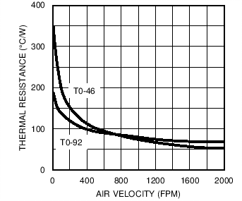 Figure 1. Thermal Resistance Junction To Air
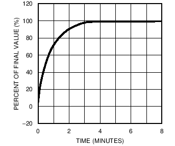 Figure 3. Thermal Response In Still Air
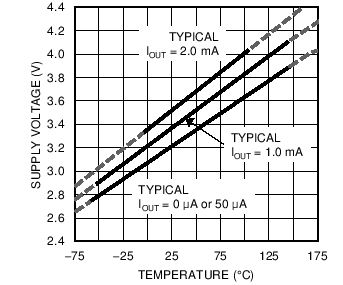 Figure 5. Minimum Supply Voltage vs Temperature
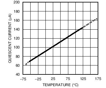 Figure 7. Quiescent Current vs Temperature (in Circuit of Full-Range Centigrade Temperature Sensor)
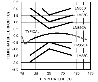 Figure 9. Accuracy vs Temperature (Ensured)
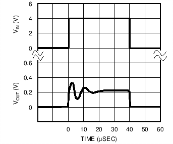 Figure 11. Start-Up Response
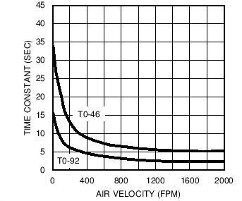 Figure 2. Thermal Time Constant
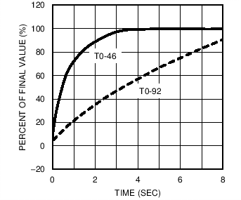 Figure 4. Thermal Response In Stirred Oil Bath
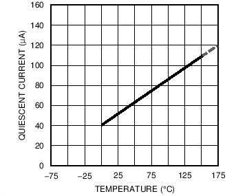 Figure 6. Quiescent Current vs Temperature (in Circuit of Figure 14)
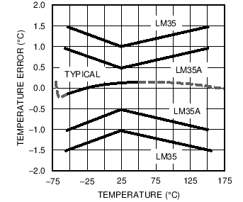 Figure 8. Accuracy vs Temperature (Ensured)
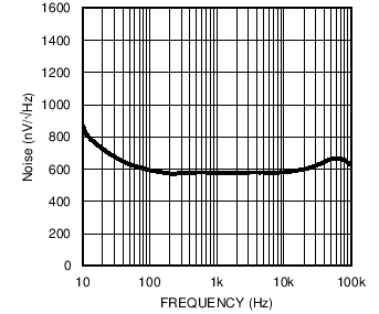 Figure 10. Noise Voltage
7 Detailed Description
7.1 Overview
The LM35-series devices are precision integrated-circuit temperature sensors, with an output voltage linearly proportional to the Centigrade temperature. The LM35 device has an advantage over linear temperature sensors calibrated in Kelvin, as the user is not required to subtract a large constant voltage from the output to obtain convenient Centigrade scaling. The LM35 device does not require any external calibration or trimming to provide typical accuracies of ± ¼ °C at room temperature and ± ¾ °C over a full −55°C to 150°C temperature range. Lower cost is assured by trimming and calibration at the wafer level. The low output impedance, linear output, and precise inherent calibration of the LM35 device makes interfacing to readout or control circuitry especially easy. The device is used with single power supplies, or with plus and minus supplies. As the LM35 device draws only 60 μA from the supply, it has very low self-heating of less than 0.1°C in still air. The LM35 device is rated to operate over a −55°C to 150°C temperature range, while the LM35C device is rated for a −40°C to 110°C range (−10° with improved accuracy). The temperature-sensing element is comprised of a delta-V BE architecture.
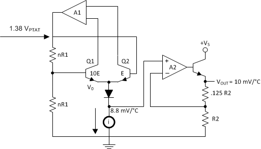
The temperature-sensing element is then buffered by an amplifier and provided to the VOUT pin. The amplifier has a simple class A output stage with typical 0.5-Ω output impedance as shown in the Functional Block Diagram. Therefore the LM35 can only source current and it's sinking capability is limited to 1 μA.
7.2 Functional Block Diagram
7.3 Feature Description
7.4 Device Functional Modes
The only functional mode of the LM35 is that it has an analog output directly proportional to temperature.