-
LM5022-Q1 2.2MHz, 60 V Low-Side Controller For Boost and SEPIC
- 1 Features
- 2 Applications
- 3 Description
- 4 Revision History
- 5 Pin Configuration and Functions
- 6 Specifications
- 7 Detailed Description
-
8 Application and Implementation
- 8.1 Application Information
- 8.2
Typical Application
- 8.2.1 Design Requirements
- 8.2.2
Detailed Design Procedure
- 8.2.2.1 Switching Frequency
- 8.2.2.2 MOSFET
- 8.2.2.3 Output Diode
- 8.2.2.4 Boost Inductor
- 8.2.2.5 Output Capacitor
- 8.2.2.6 VCC Decoupling Capacitor
- 8.2.2.7 Input Capacitor
- 8.2.2.8 Current Sense Filter
- 8.2.2.9 RSNS, RS2 and Current Limit
- 8.2.2.10 Control Loop Compensation
- 8.2.2.11 Efficiency Calculations
- 8.2.3 Application Curves
- 9 Power Supply Recommendations
- 10Layout
- 11Device and Documentation Support
- 12Mechanical, Packaging, and Orderable Information
- IMPORTANT NOTICE
Package Options
Mechanical Data (Package|Pins)
- DGS|10
Thermal pad, mechanical data (Package|Pins)
Orderable Information
LM5022-Q1 2.2MHz, 60 V Low-Side Controller For Boost and SEPIC
1 Features
- AEC-Q100 Grade 1 Qualified with the following results:
- Device Temperature Grade 1: -40°C to 125°C Ambient Operating Temperature Range
- Device HBM ESD Classification Level 2
- Device CDM ESD Classification Level C5
- Internal 60-V Start-Up Regulator
- 1-A Peak MOSFET Gate Driver
- VIN Range: 6 V to 60 V (operate down to 3 V after startup)
- Duty Cycle Limit of 90%
- Programmable UVLO with Hysteresis
- Cycle-by-Cycle Current Limit
- Single Resistor Oscillator Frequency Set
- Adjustable Switching Frequency to 2.2MHz
- External Clock Synchronization
- Slope Compensation
- Adjustable Soft Start
- 10-Pin VSSOP Package
2 Applications
- Boost Converter
- SEPIC Converter
3 Description
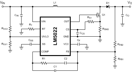
The LM5022-Q1 is a high voltage low-side N-channel MOSFET controller ideal for use in boost and SEPIC regulators. It contains all of the features needed to implement single-ended primary topologies. Output voltage regulation is based on current-mode control, which eases the design of loop compensation while providing inherent input voltage feed-forward. The LM5022-Q1 includes a start-up regulator that operates over a wide input range of 6 V to 60 V. The PWM controller is designed for high-speed capability including an oscillator frequency range up to 2.2 MHz and total propagation delays less than 100 ns. Additional features include an error amplifier, precision reference, line undervoltage lockout, cycle-by-cycle current limit, slope compensation, soft-start, external synchronization capability, and thermal shutdown. The LM5022-Q1 is available in the 10-pin VSSOP package.
Device Information(1)
| PART NUMBER | PACKAGE | BODY SIZE (NOM) |
|---|---|---|
| LM5022-Q1 | VSSOP (10) | 3.00 mm × 3.00 mm |
- For all available packages, see the orderable addendum at the end of the data sheet.
Typical Application
4 Revision History
| DATE | REVISION | NOTES |
|---|---|---|
| March 2016 | * | Initial release. |
5 Pin Configuration and Functions
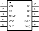
Pin Functions
| PIN | TYPE | DESCRIPTION | APPLICATION INFORMATION | |
|---|---|---|---|---|
| NO. | NAME | |||
| 1 | VIN | I | Source input voltage | Input to the start-up regulator. Operates from 6 V to 60 V. |
| 2 | FB | I | Feedback pin | Inverting input to the internal voltage error amplifier. The non-inverting input of the error amplifier connects to a 1.25-V reference. |
| 3 | COMP | I/O | Error amplifier output and PWM comparator input | The control loop compensation components connect between this pin and the FB pin. |
| 4 | VCC | O | Output of the internal, high voltage linear regulator. | This pin should be bypassed to the GND pin with a ceramic capacitor. |
| 5 | OUT | O | Output of MOSFET gate driver | Connect this pin to the gate of the external MOSFET. The gate driver has a 1-A peak current capability. |
| 6 | GND | - | System ground | |
| 7 | UVLO | I | Input undervoltage lockout | Set the start-up and shutdown levels by connecting this pin to the input voltage through a resistor divider. A 20-µA current source provides hysteresis. |
| 8 | CS | I | Current sense input | Input for the switch current used for current mode control and for current limiting. |
| 9 | RT/SYNC | I | Oscillator frequency adjust pin and synchronization input | An external resistor connected from this pin to GND sets the oscillator frequency. This pin can also accept an AC-coupled input for synchronization from an external clock. |
| 10 | SS | I | Soft-start pin | An external capacitor placed from this pin to ground will be charged by a 10-µA current source, creating a ramp voltage to control the regulator start-up. |
6 Specifications
6.1 Absolute Maximum Ratings
over operating free-air temperature range (unless otherwise noted)(1)(2)| MIN | MAX | UNIT | ||
|---|---|---|---|---|
| VIN to GND | –0.3 | 65 | V | |
| VCC to GND | –0.3 | 16 | V | |
| RT/SYNC to GND | –0.3 | 5.5 | V | |
| OUT to GND | –1.5V for < 100 ns | |||
| All other pins to GND | –0.3 | 7 | V | |
| Power dissipation | Internally limited | |||
| Junction temperature(3) | 150 | °C | ||
| Soldering information | Vapor phase (60 sec.) | 215 | °C | |
| Infrared (15 sec.) | 220 | °C | ||
| Storage temperature, Tstg | –65 | 150 | °C | |
6.2 ESD Ratings: LM5022-Q1
| VALUE | UNIT | |||
|---|---|---|---|---|
| V(ESD) | Human body model (HBM), per AEC Q100-002(1) | ±2000 | V | |
| Charged device model (CDM), per AEC Q100-011(2) | ±750 | V | ||
6.3 Recommended Operating Conditions
over operating free-air temperature range (unless otherwise noted)(1)| MIN | NOM | MAX | UNIT | ||
|---|---|---|---|---|---|
| Supply voltage | 6 | 60 | V | ||
| External voltage at VCC | 7.5 | 14 | V | ||
| Junction temperature | –40 | 125 | °C | ||
6.4 Thermal Information
| THERMAL METRIC(1) | LM5022-Q1 | UNIT | |
|---|---|---|---|
| DGS (VSSOP) | |||
| 10 PINS | |||
| RθJA | Junction-to-ambient thermal resistance | 161.5 | °C/W |
| RθJC(top) | Junction-to-case (top) thermal resistance | 56 | °C/W |
| RθJB | Junction-to-board thermal resistance | 81.3 | °C/W |
| ψJT | Junction-to-top characterization parameter | 5.7 | °C/W |
| ψJB | Junction-to-board characterization parameter | 80 | °C/W |
| RθJC(bot) | Junction-to-case (bottom) thermal resistance | N/A | °C/W |
6.5 Electrical Characteristics
Typical limits apply for TJ = 25°C and are provided for reference purposes only; minimum and maximum limits apply over the junction temperature (TJ) range of –40°C to +125°C. VIN = 24 V and RT = 27.4 kΩ, unless otherwise indicated.(1)| PARAMETER | TEST CONDITIONS | MIN | TYP | MAX | UNIT | |
|---|---|---|---|---|---|---|
| SYSTEM PARAMETERS | ||||||
| VFB | FB Pin Voltage | 1.225 | 1.250 | 1.275 | V | |
| START-UP REGULATOR | ||||||
| VCC(2) | VCC Regulation | 10 V ≤ VIN ≤ 60 V, ICC = 1 mA | 6.6 | 7 | 7.4 | V |
| VCC Regulation | 6 V ≤ VIN < 10 V, VCC Pin Open Circuit | 5 | ||||
| ICC | Supply Current | OUT Pin Capacitance = 0 VCC = 10 V |
3.5 | 4 | mA | |
| ICC-LIM | VCC Current Limit | VCC = 0 V, ((3), (2)) | 15 | 35 | mA | |
| VIN - VCC | Dropout Voltage Across Bypass Switch | ICC = 0 mA, ƒSW < 200 kHz 6 V ≤ VIN ≤ 8.5 V |
200 | mV | ||
| VBYP-HI | Bypass Switch Turn-off Threshold | VIN increasing | 8.7 | V | ||
| VBYP-HYS | Bypass Switch Threshold Hysteresis | VIN Decreasing | 260 | mV | ||
| ZVCC | VCC Pin Output Impedance 0 mA ≤ ICC ≤ 5 mA |
VIN = 6 V | 58 | Ω | ||
| VIN = 8 V | 53 | |||||
| VIN = 24 V | 1.6 | |||||
| VCC-HI | VCC Pin UVLO Rising Threshold | 5 | V | |||
| VCC-HYS | VCC Pin UVLO Falling Hysteresis | 300 | mV | |||
| IVIN | Start-up Regulator Leakage | VIN = 60 V | 150 | 500 | µA | |
| IIN-SD | Shutdown Current | VUVLO = 0 V, VCC = Open Circuit | 350 | 450 | µA | |
| ERROR AMPLIFIER | ||||||
| GBW | Gain Bandwidth | 4 | MHz | |||
| ADC | DC Gain | 75 | dB | |||
| ICOMP | COMP Pin Current Sink Capability | VFB = 1.5 V VCOMP = 1 V |
5 | 17 | mA | |
| UVLO | ||||||
| VSD | Shutdown Threshold | 1.22 | 1.25 | 1.28 | V | |
| ISD-HYS | Shutdown Hysteresis Current Source |
16 | 20 | 24 | µA | |
| CURRENT LIMIT | ||||||
| tLIM-DLY | Delay from ILIM to Output | CS steps from 0 V to 0.6 V OUT transitions to 90% of VCC |
30 | ns | ||
| VCS | Current Limit Threshold Voltage | 0.434 | 0.5 | 0.55 | V | |
| tBLK | Leading Edge Blanking Time | 65 | ns | |||
| RCS | CS Pin Sink Impedance | Blanking active | 40 | 75 | Ω | |
| SOFT-START | ||||||
| ISS | Soft-start Current Source | 7 | 10 | 13 | µA | |
| VSS-OFF | Soft-start to COMP Offset | 0.344 | 0.55 | 0.75 | V | |
| OSCILLATOR | ||||||
| fSW | RT to GND = 84.5 kΩ | See(4) | 170 | 200 | 230 | kHz |
| RT to GND = 27.4 kΩ | See(4) | 525 | 600 | 675 | kHz | |
| RT to GND = 16.2 kΩ | See(4) | 865 | 990 | 1115 | kHz | |
| RT to GND = 6.65 kΩ | See(4) | 1910 | 2240 | 2570 | kHz | |
| VSYNC-HI | Synchronization Rising Threshold | 3.8 | V | |||
| PWM COMPARATOR | ||||||
| tCOMP-DLY | Delay from COMP to OUT Transition | VCOMP = 2 V CS stepped from 0 V to 0.4 V |
25 | ns | ||
| DMIN | Minimum Duty Cycle | VCOMP = 0 V | 0% | |||
| DMAX | Maximum Duty Cycle | 90% | 95% | |||
| APWM | COMP to PWM Comparator Gain | 0.33 | V/V | |||
| VCOMP-OC | COMP Pin Open Circuit Voltage | VFB = 0 V | 4.3 | 5.2 | 6.1 | V |
| ICOMP-SC | COMP Pin Short Circuit Current | VCOMP = 0 V, VFB = 0V | 0.6 | 1.1 | 1.5 | mA |
| SLOPE COMPENSATION | ||||||
| VSLOPE | Slope Compensation Amplitude | 83 | 110 | 137 | mV | |
| MOSFET DRIVER | ||||||
| VSAT-HI | Output High Saturation Voltage (VCC – VOUT) | IOUT = 50 mA | 0.25 | 0.75 | V | |
| VSAT-LO | Output Low Saturation Voltage (VOUT) | IOUT = 100 mA | 0.25 | 0.75 | V | |
| tRISE | OUT Pin Rise Time | OUT Pin load = 1 nF | 18 | ns | ||
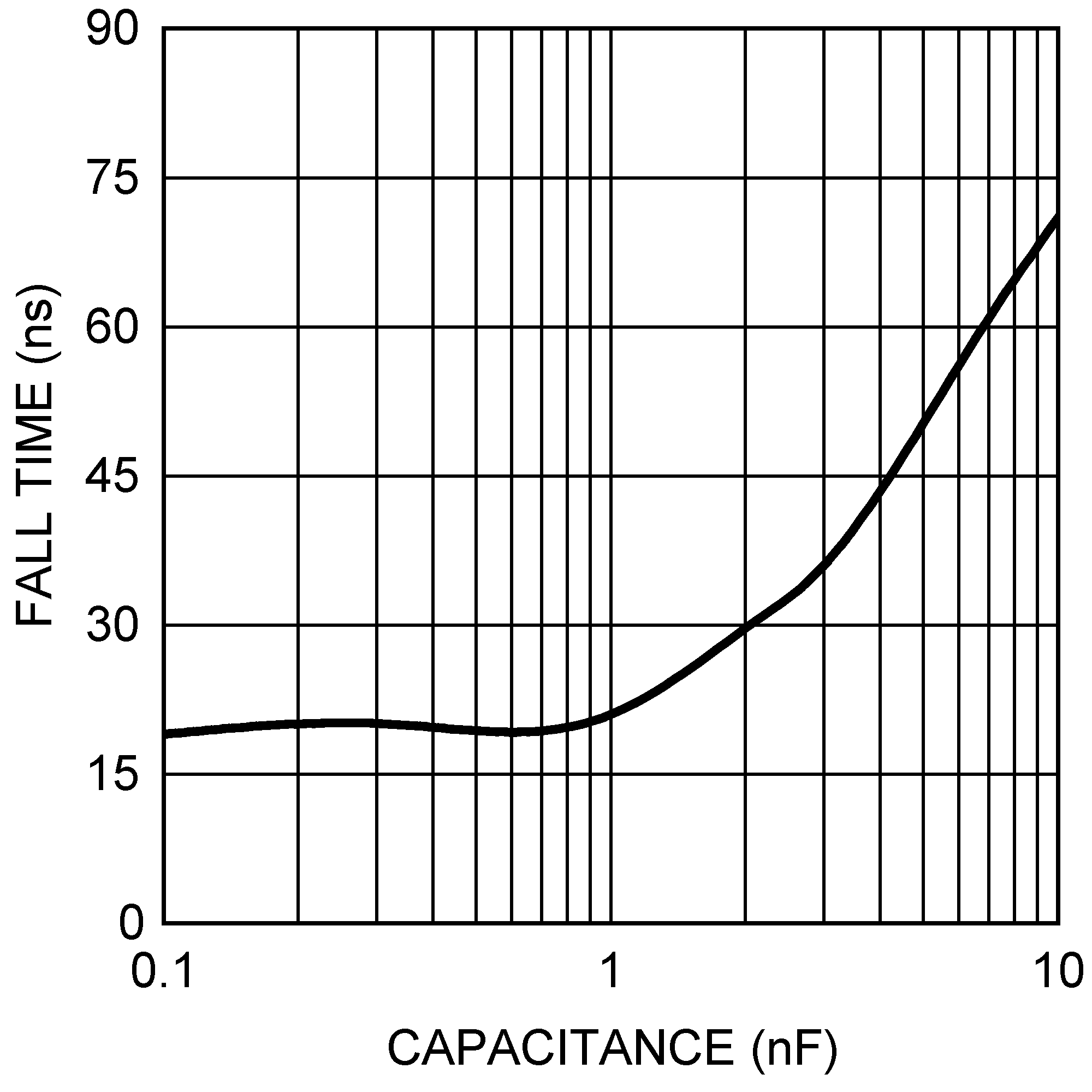
| tFALL | OUT Pin Fall Time | OUT Pin load = 1 nF | 15 | ns | ||
| THERMAL CHARACTERISTICS | ||||||
| TSD | Thermal Shutdown Threshold | 165 | °C | |||
| TSD-HYS | Thermal Shutdown Hysteresis | 25 | °C | |||
6.6 Typical Characteristics

| VO = 40 V |
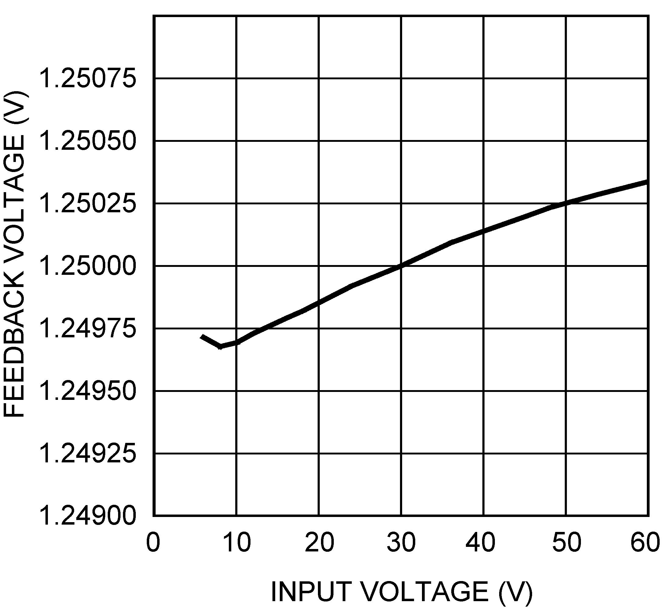
| TA = 25°C |
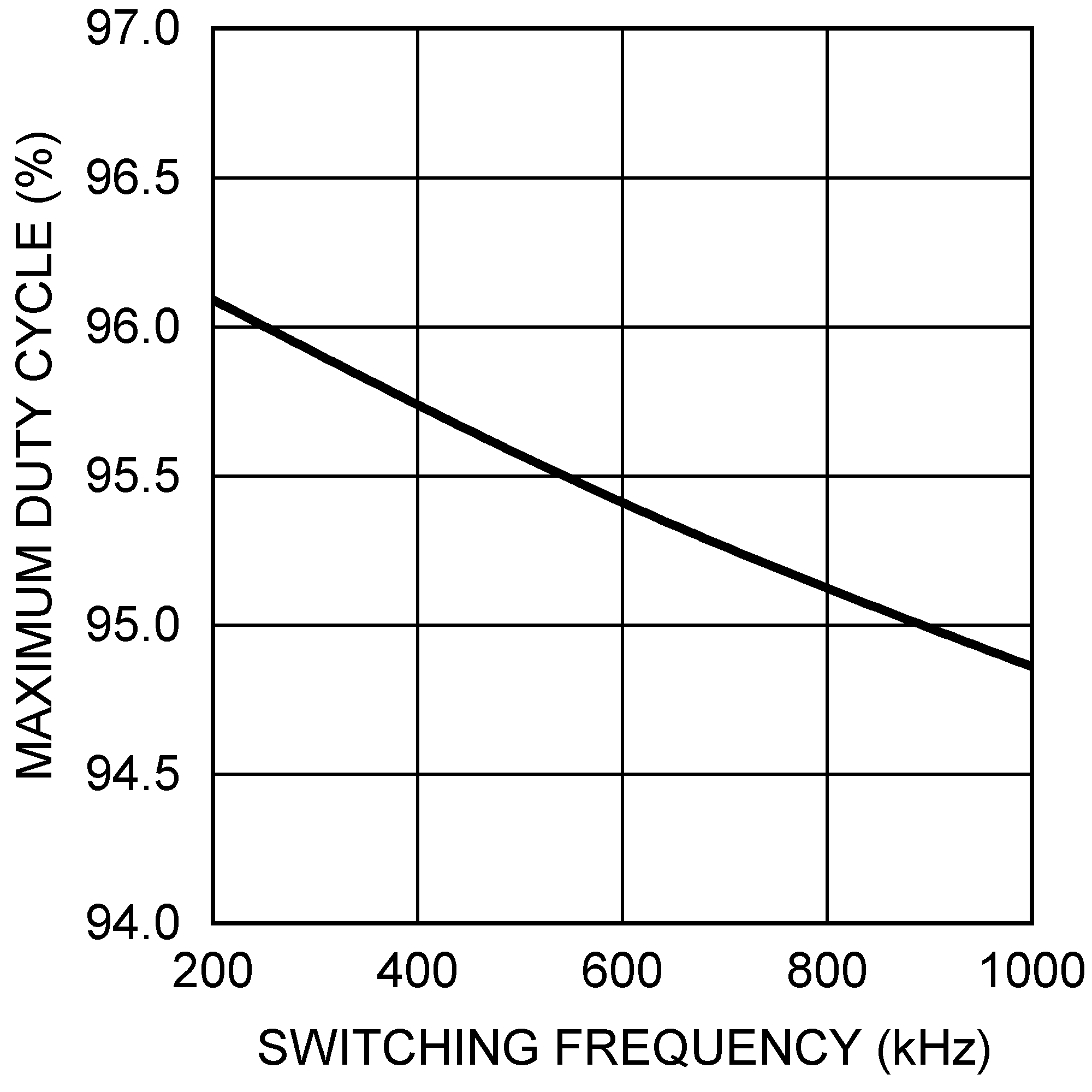
| TA = 25°C |

| RT = 6.65 KΩ | ||
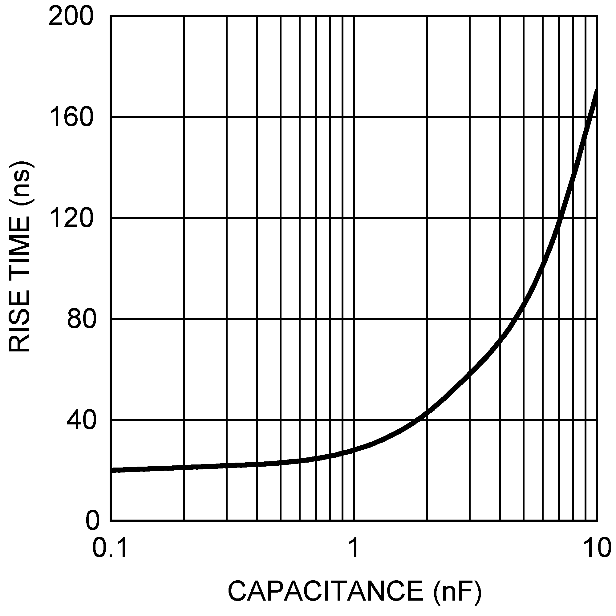

| TA = 25°C |
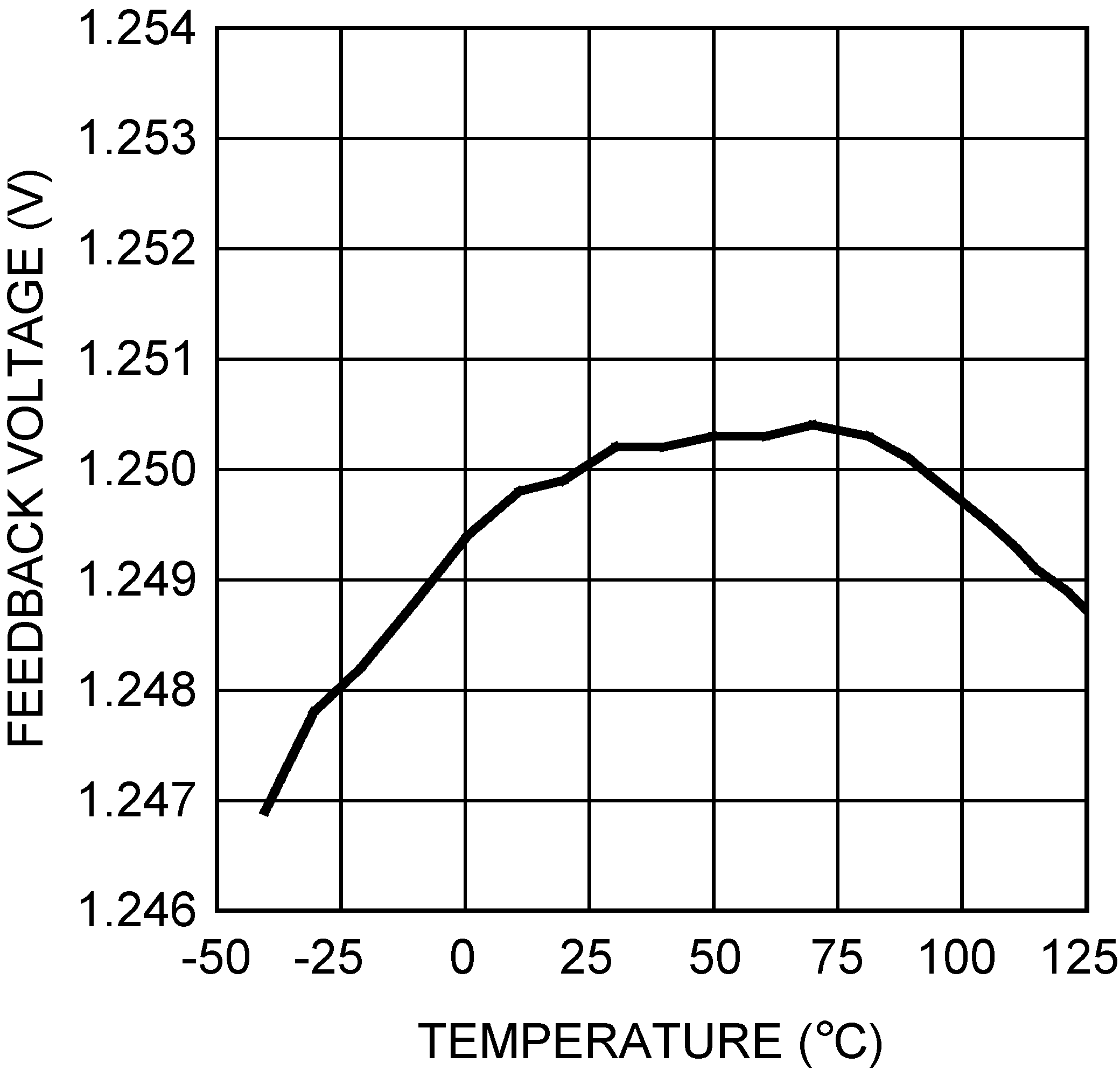
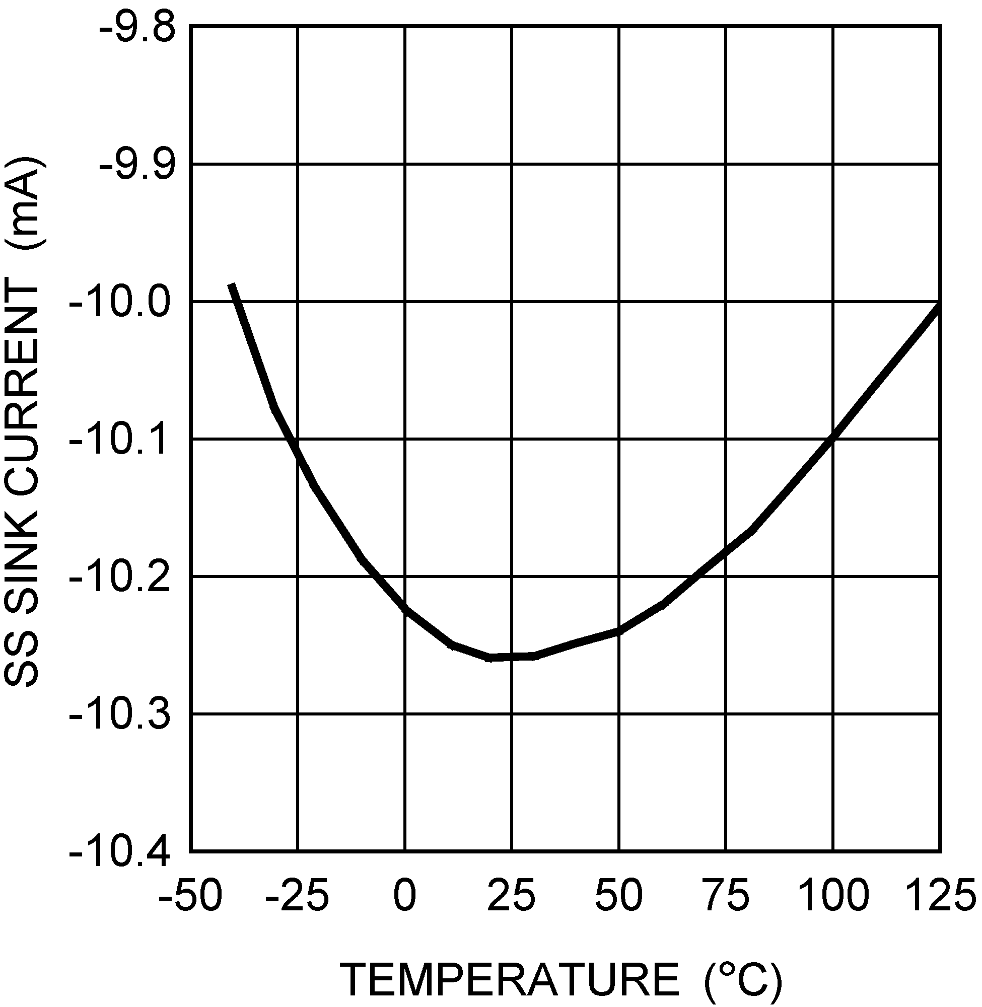
| VIN = 24 V |
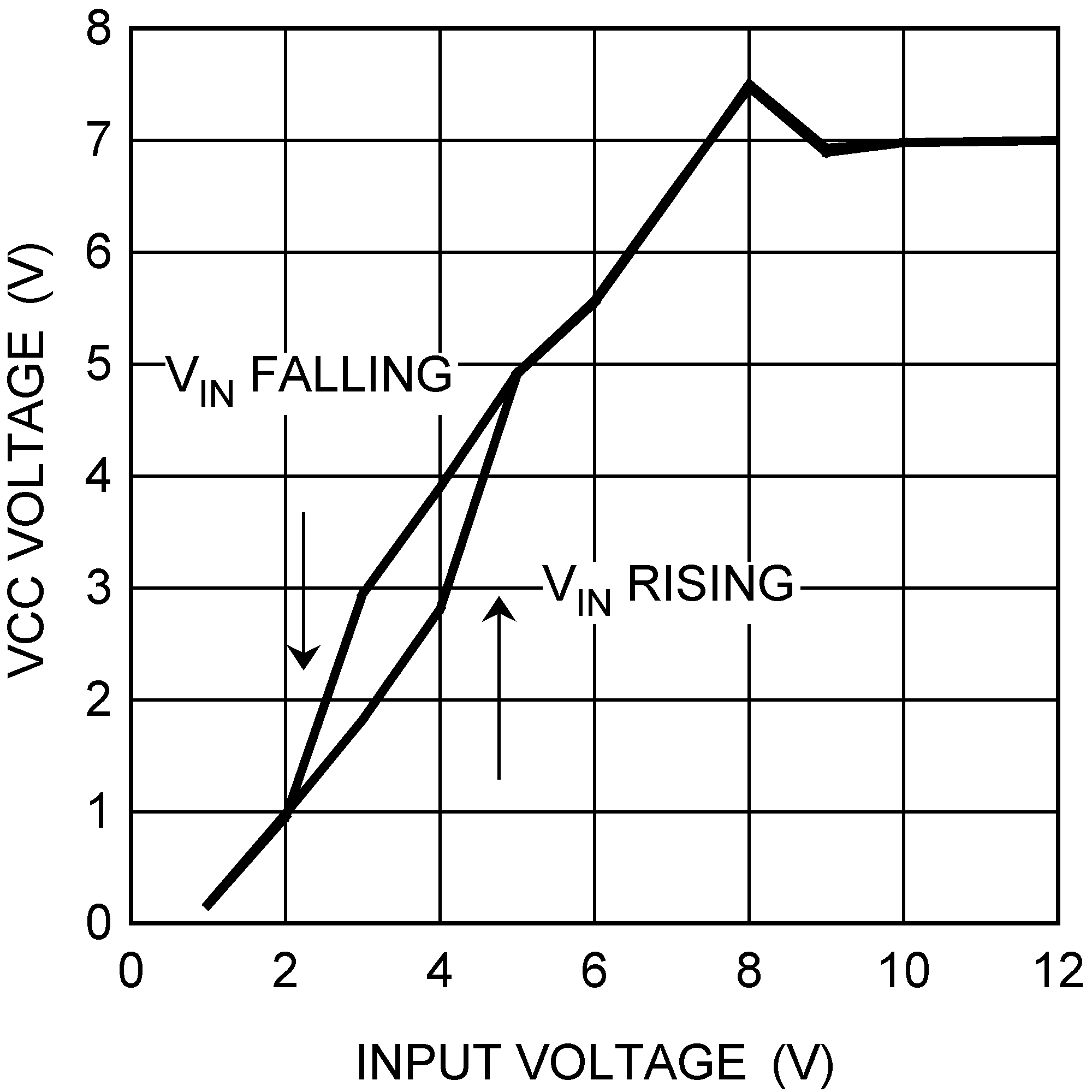
| TA = 25°C |
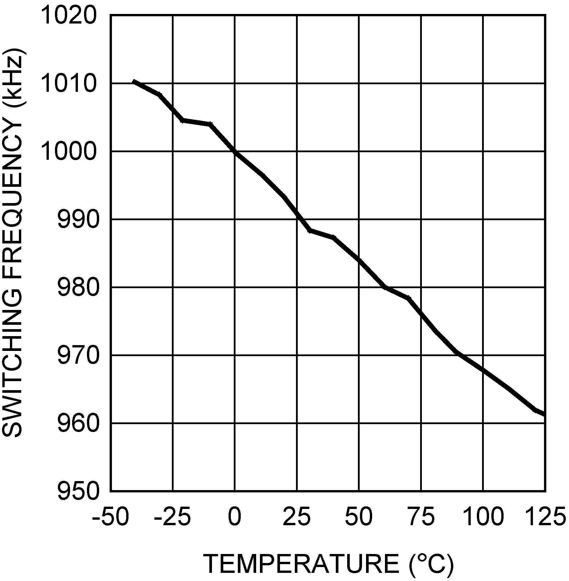
| RT = 16.2 KΩ |
