-
LM5134 Single 7.6-A Peak Current Low-Side Gate Driver With a PILOT Output
- 1 Features
- 2 Applications
- 3 Description
- 4 Revision History
- 5 Pin Configuration and Functions
- 6 Specifications
- 7 Detailed Description
- 8 Application and Implementation
- 9 Power Supply Recommendations
- 10Layout
- 11Device and Documentation Support
- 12Mechanical, Packaging, and Orderable Information
- IMPORTANT NOTICE
Package Options
Mechanical Data (Package|Pins)
Thermal pad, mechanical data (Package|Pins)
Orderable Information
LM5134 Single 7.6-A Peak Current Low-Side Gate Driver With a PILOT Output
1 Features
- 7.6-A and 4.5-A Peak Sink and Source Drive Current for Main Output
- 820-mA and 660-mA Peak Sink and Source Current for PILOT Output
- 4-V to 12.6-V Single-Power Supply
- Matching Delay Time Between Inverting and Non-Inverting Inputs
- TTL/CMOS Logic Inputs
- Up to 14-V Logic Inputs (Regardless of VDD Voltage)
- –40°C to 125°C Junction Temperature Range
2 Applications
- Motor Drivers
- Solid-State Power Controllers
- Power Factor Correction Converters
3 Description
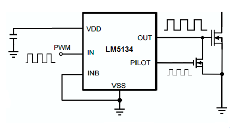
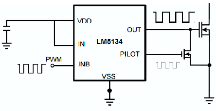
The LM5134 is a high-speed single low-side driver capable of sinking and sourcing 7.6-A and 4.5-A peak currents. The LM5134 has inverting and noninverting inputs that give the user greater flexibility in controlling the FET. The LM5134 features one main output, OUT, and an extra gate drive output, PILOT. The PILOT pin logic is complementary to the OUT pin, and can be used to drive a small MOSFET located close to the main power FET. This configuration minimizes the turnoff loop and reduces the consequent parasitic inductance. It is particularly useful for driving high-speed FETs or multiple FETs in parallel. The LM5134 is available in the 6-pin
SOT-23 package and the 6-pin WSON package with an exposed pad to aid thermal dissipation.
Device Information(1)
| PART NUMBER | PACKAGE | BODY SIZE (NOM) |
|---|---|---|
| LM5134 | SOT-23 (6) | 2.90 mm × 1.60 mm |
| WSON (6) | 3.00 mm × 3.00 mm |
- For all available packages, see the orderable addendum at the end of the data sheet.
Noninverting Input
Inverting Input
4 Revision History
Changes from B Revision (April 2013) to C Revision
- Added ESD Ratings table, Feature Description section, Device Functional Modes section, Application and Implementation section, Power Supply Recommendations section, Layout section, Device and Documentation Support section, and Mechanical, Packaging, and Orderable Information section. Go
Changes from A Revision (April 2013) to B Revision
- Changed layout of National Data Sheet to TI formatGo
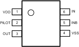
5 Pin Configuration and Functions
Pin Functions
| PIN | I/O | DESCRIPTION | APPLICATION INFORMATION | |
|---|---|---|---|---|
| NAME | NO. | |||
| VDD | 1 | — | Gate drive supply | Locally decouple to VSS using low ESR/ESL capacitor located as close as possible to the IC. |
| PILOT | 2 | O | Gate drive output for an external turnoff FET | Connect to the gate of a small turnoff MOSFET with a short, low inductance path. The turnoff FET provides a local turnoff path. |
| OUT | 3 | O | Gate drive output for the power FET | Connect to the gate of the power FET with a short, low inductance path. A gate resistor can be used to eliminate potential gate oscillations. |
| VSS | 4 | — | Ground | All signals are referenced to this ground. |
| INB | 5 | I | Inverting logic input | Connect to VSS when not used. |
| IN | 6 | I | Non-inverting logic input | Connect to VDD when not used. |
| EP | EP | — | Exposed Pad | It is recommended that the exposed pad on the bottom of the package be soldered to ground plane on the PC board, and that ground plane extend out from beneath the IC to help dissipate heat. |
6 Specifications
6.1 Absolute Maximum Ratings
over operating free-air temperature range (unless otherwise noted)(1)| MIN | MAX | UNIT | ||
|---|---|---|---|---|
| Pin voltage | VDD to VSS | −0.3 | 14 | V |
| IN, INB to VSS | −0.3 | 14 | ||
| Junction temperature, TJ | 150 | °C | ||
| Storage temperature, Tstg | −55 | 150 | °C | |
6.2 ESD Ratings
| VALUE | UNIT | |||
|---|---|---|---|---|
| V(ESD) | Electrostatic discharge | Human-body model (HBM), per ANSI/ESDA/JEDEC JS-001(1) | ±2000 | V |
| Charged-device model (CDM), per JEDEC specification JESD22-C101(2) | ±1000 | |||
6.3 Recommended Operating Conditions
over operating free-air temperature range (unless otherwise noted)| MIN | NOM | MAX | UNIT | |
|---|---|---|---|---|
| Gate drive supply, VDD | 4 | 12.6 | V | |
| Operating junction temperature | –40 | 125 | °C |
6.4 Thermal Information
| THERMAL METRIC(1) | LM5134 | UNIT | ||
|---|---|---|---|---|
| DBV (SOT-23) | NGG (WSON) | |||
| 6 PINS | 6 PINS | |||
| RθJA | Junction-to-ambient thermal resistance | 105.9 | 51 | °C/W |
| RθJC(top) | Junction-to-case (top) thermal resistance | 52.1 | 47 | °C/W |
| RθJB | Junction-to-board thermal resistance | 21 | 25.3 | °C/W |
| ψJT | Junction-to-top characterization parameter | 1.2 | 0.6 | °C/W |
| ψJB | Junction-to-board characterization parameter | 20.5 | 24.5 | °C/W |
| RθJC(bot) | Junction-to-case (bottom) thermal resistance | N/A | 5.8 | °C/W |
6.5 Electrical Characteristics
TJ = 25°C, VDD = 12 V, unless otherwise specified. Minimum and Maximum limits are ensured through test, design, or statistical correlation. Typical values represent the most likely parametric norm at TJ = 25°C, and are provided for reference purposes only.(1).| PARAMETER | TEST CONDITIONS | MIN | TYP | MAX | UNIT | ||
|---|---|---|---|---|---|---|---|
| POWER SUPPLY | |||||||
| VDD | VDD operating voltage | TJ = –40°C to +125°C | 4 | 12.6 | V | ||
| UVLO | VDD undervoltage lockout | VDD rising | TJ = 25°C | 3.6 | V | ||
| TJ = –40°C to +125°C | 3.25 | 4 | |||||
| VDD undervoltage lockout hysteresis | 0.36 | V | |||||
| VDD undervoltage lockout to main output delay time | VDD rising | 500 | ns | ||||
| IDD | VDD quiescent current | IN = INB = VDD | TJ = 25°C | 0.8 | mA | ||
| TJ = –40°C to +125°C | 2 | ||||||
| OUTPUT | |||||||
| RON-DW (SOT23-6) | Main output resistance – pulling down | VDD = 10 V, IOUT = –100 mA | TJ = 25°C | 0.15 | Ω | ||
| TJ = –40°C to +125°C | 0.45 | ||||||
| VDD = 4.5 V, IOUT = –100 mA | TJ = 25°C | 0.2 | Ω | ||||
| TJ = –40°C to +125°C | 0.5 | ||||||
| RON-DW (WSON) | Main output resistance – pulling down | VDD = 10 V, IOUT = –100 mA | TJ = 25°C | 0.2 | Ω | ||
| TJ = –40°C to +125°C | 0.5 | ||||||
| VDD = 4.5 V, IOUT = –100 mA | TJ = 25°C | 0.25 | Ω | ||||
| TJ = –40°C to +125°C | 0.55 | ||||||
| Power-off pulldown resistance | VDD = 0 V, IOUT = –10 mA | 1.5 | 10 | Ω | |||
| Power-off pulldown clamp voltage | VDD = 0 V, IOUT = –10 mA | 0.7 | 1 | V | |||
| Peak sink current | CL = 10,000 pF | 7.6 | A | ||||
| RON-UP (SOT23-6) | Main output resistance - pulling up | VDD = 10 V, IOUT = 50 mA |
TJ = 25°C | 0.7 | Ω | ||
| TJ = –40°C to +125°C | 1.3 | ||||||
| VDD = 4.5 V, IOUT = 50 mA |
TJ = 25°C | 1 | Ω | ||||
| TJ = –40°C to +125°C | 1.9 | ||||||
| RON-UP (WSON) | Main output resistance - pulling up | VDD = 10 V, IOUT = 50 mA |
TJ = 25°C | 0.75 | Ω | ||
| TJ = –40°C to +125°C | 1.2 | ||||||
| VDD = 4.5 V, IOUT = 50 mA |
TJ = 25°C | 1.14 | Ω | ||||
| TJ = –40°C to +125°C | 1.85 | ||||||
| Peak source current | CL = 10,000 pF | 4.5 | A | ||||
| PILOT | |||||||
| RONP-DW | PILOT output resistance – pulling down | VDD = 10 V, IOUT = –100 mA |
TJ = 25°C | 3.7 | Ω | ||
| TJ = –40°C to +125°C | 9 | ||||||
| VDD = 4.5 V, IOUT = –100 mA |
TJ = 25°C | 4.7 | Ω | ||||
| TJ = –40°C to +125°C | 12 | ||||||
| Peak sink current | CL = 330 pF | 820 | mA | ||||
| RONP-UP | PILOT output resistance – pulling up | VDD = 10 V, IOUT = 50 mA |
TJ = 25°C | 6 | Ω | ||
| TJ = –40°C to +125°C | 11 | ||||||
| VDD = 4.5 V, IOUT = 50 mA |
TJ = 25°C | 10.7 | Ω | ||||
| TJ = –40°C to +125°C | 20 | ||||||
| Peak source current | CL = 330 pF | 660 | mA | ||||
| LOGIC INPUT | |||||||
| VIH | Logic 1 input voltage | LM5134A, TJ = –40°C to +125°C | 0.67 × VDD | V | |||
| LM5134B, TJ = –40°C to +125°C | 2.4 | ||||||
| VIL | Logic 0 input voltage | LM5134A, TJ = –40°C to +125°C | 0.33 × VDD | V | |||
| LM5134B, TJ = –40°C to +125°C | 0.8 | ||||||
| VHYS | Logic-input hysteresis | LM5134A | 0.9 | V | |||
| LM5134B | 0.68 | ||||||
| Logic-input current | INB = VDD or 0 | TJ = 25°C | 0.001 | µA | |||
| TJ = –40°C to +125°C | 10 | ||||||
| THERMAL RESISTANCE | |||||||
| θJA | Junction to ambient | SOT23-6 | 90 | °C/W | |||
| WSON-6 | 60 | °C/W | |||||
6.6 Switching Characteristics
over operating free-air temperature range (unless otherwise noted)| PARAMETER | TEST CONDITIONS | MIN | TYP | MAX | UNIT | ||
|---|---|---|---|---|---|---|---|
| FOR VDD = +10 V | |||||||
| tR | OUT rise time | CL = 1000 pF | 3 | ns | |||
| CL = 5000 pF | 10 | ||||||
| CL = 10,000 pF | 20 | ||||||
| tF | OUT fall time | CL = 1000 pF | 2 | ns | |||
| CL = 5000 pF | 4.7 | ||||||
| CL = 10,000 pF | 7.2 | ||||||
| tD-ON | OUT turnon propagation delay | CL = 1000 pF | TJ = 25°C | 17 | ns | ||
| TJ = –40°C to +125°C | 40 | ||||||
| tD-OFF | OUT turnoff propagation delay | CL = 1000 pF | TJ = 25°C | 12 | ns | ||
| TJ = –40°C to +125°C | 25 | ||||||
| Main output break-before-make time | 2.5 | ns | |||||
| tPR | PILOT rise time | CL = 330 pF | 5.3 | ns | |||
| tPF | PILOT fall time | CL = 330 pF | 3.9 | ns | |||
| tPD-ON | OUT turnoff to PILOT turnon propagation delay | CL = 330 pF | 4.2 | ns | |||
| tPD-OFF | PILOT turnoff to OUT turnon propagation delay | CL = 330 pF | 6.4 | ns | |||
| FOR VDD = +4.5 V | |||||||
| tR | Rise time | CL = 1000 pF | 5 | ns | |||
| CL = 5000 pF | 14 | ||||||
| CL = 10,000 pF | 24 | ||||||
| tF | Fall time | CL = 1000 pF | 2.3 | ns | |||
| CL = 5000 pF | 5.4 | ||||||
| CL = 10,00 0pF | 7.2 | ||||||
| tD-ON | OUT turnon propagation delay | CL = 1000 pF | TJ = 25°C | 26 | ns | ||
| TJ = –40°C to +125°C | 50 | ||||||
| tD-OFF | OUT turnoff propagation delay | CL = 1000 pF | TJ = 25°C | 20 | ns | ||
| TJ = –40°C to +125°C | 45 | ||||||
| Main output break-before-make time | 4.2 | ns | |||||
| tPR | PILOT rise time | CL = 330 pF | 9.6 | ns | |||
| tPf | PILOT fall time | CL = 330 pF | 3.7 | ns | |||
| tPD-ON | OUT turnoff to PILOT turnon propagation delay | CL = 330 pF | 7.5 | ns | |||
| tPD-OFF | PILOT turnoff to OUT turnon propagation delay | CL = 330 pF | 11.8 | ns | |||
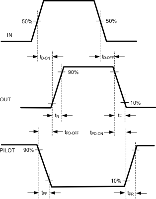 Figure 1. Timing Diagram — Noninverting Input
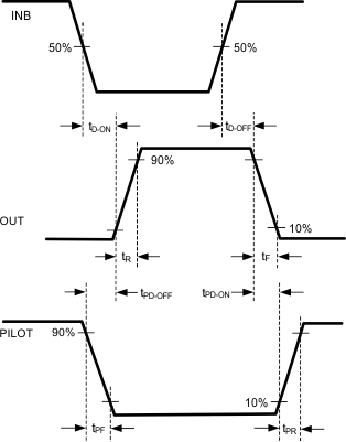 Figure 2. Timing Diagram — Inverting Input
6.7 Typical Characteristics
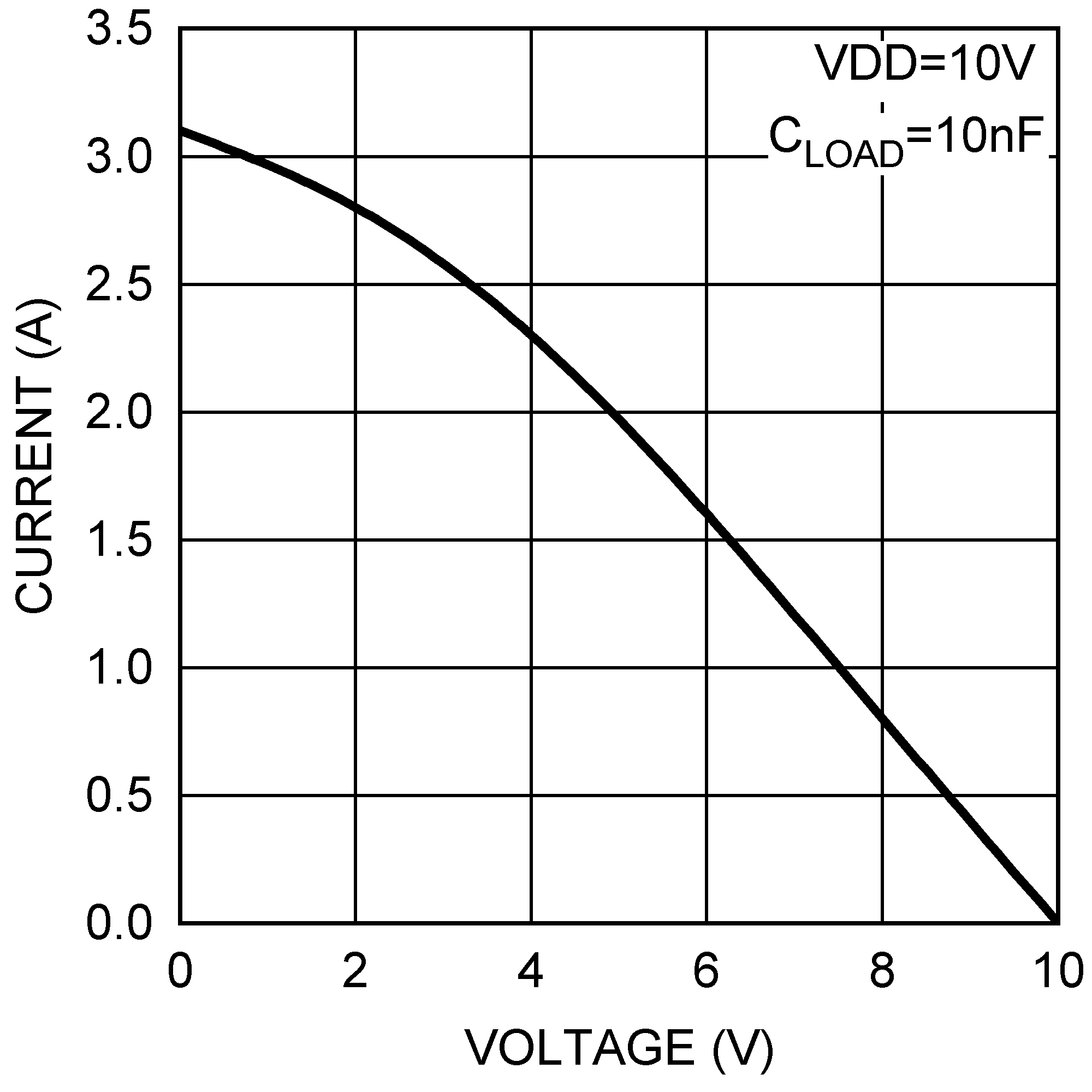 Figure 3. OUT Source Current vs OUT Voltage
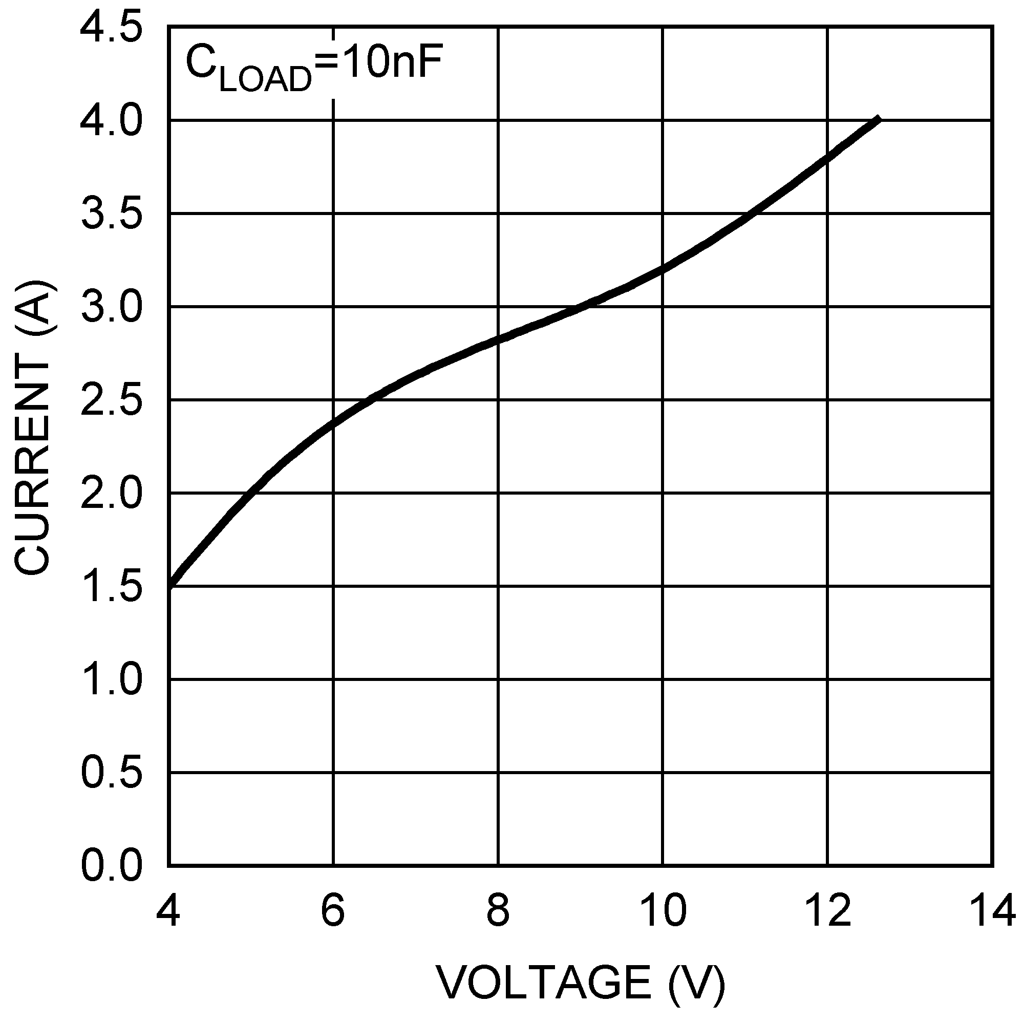 Figure 5. OUT Peak Source Current vs VDD Voltage
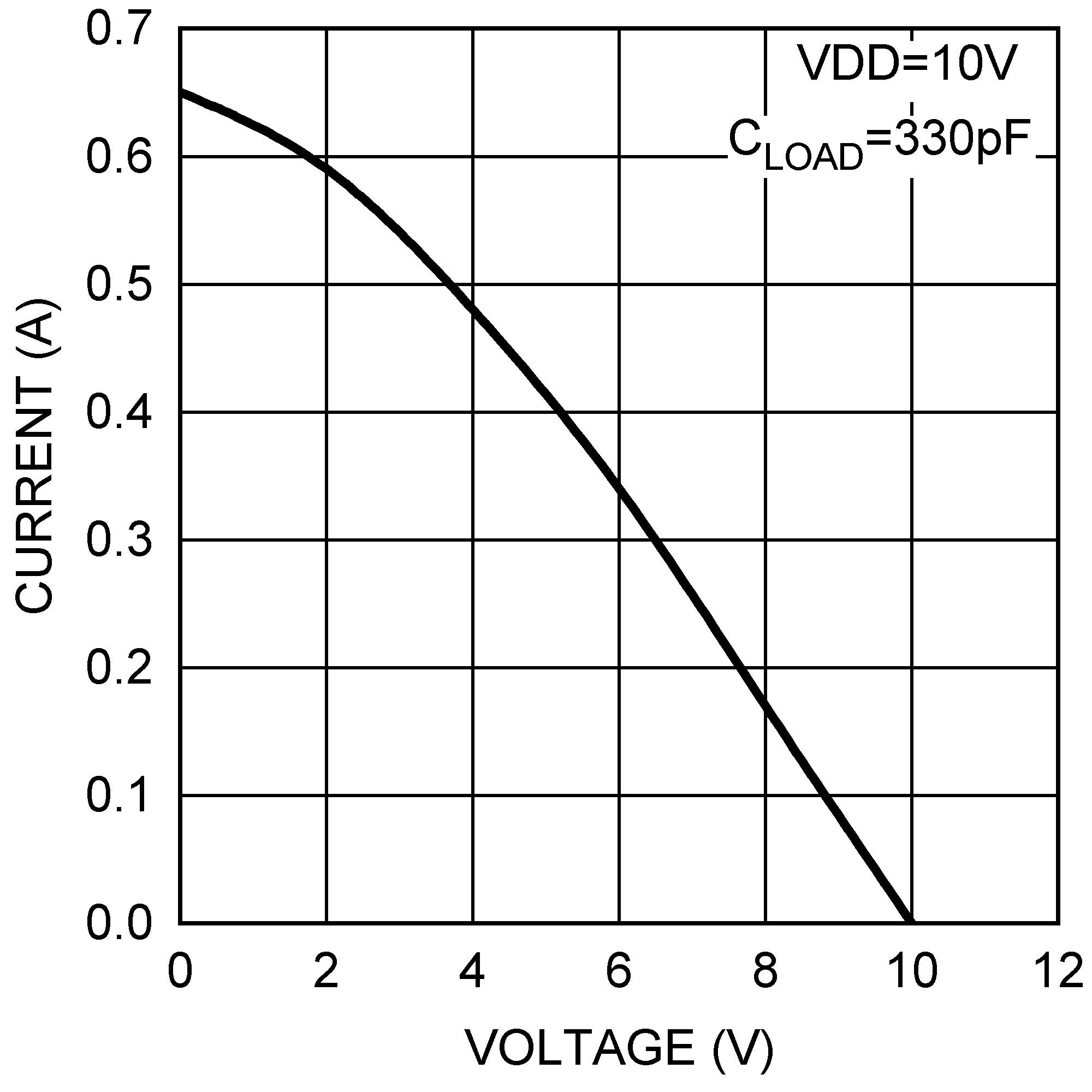 Figure 7. PILOT Source Current vs PILOT Voltage
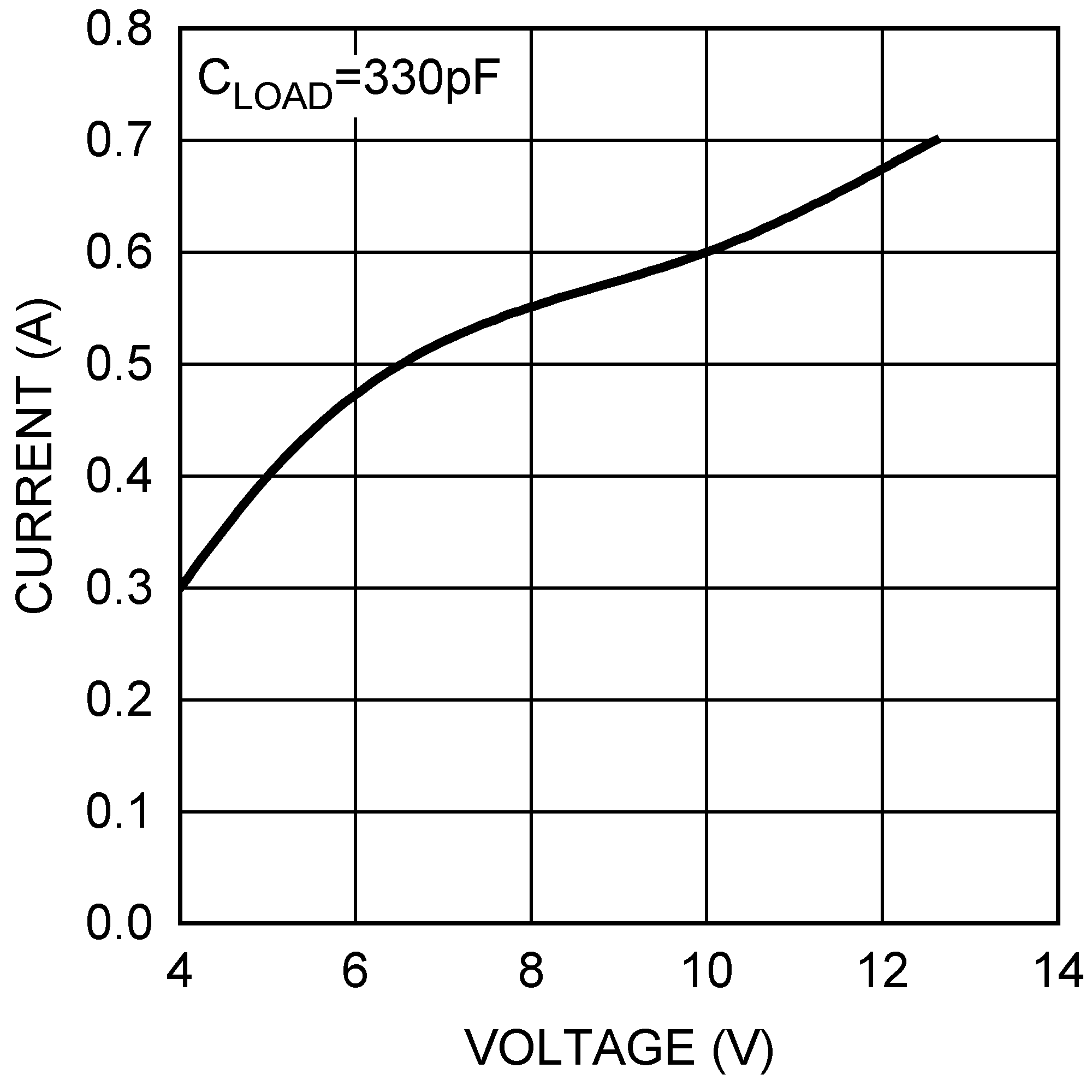 Figure 9. PILOT Peak Source Current vs VDD Voltage
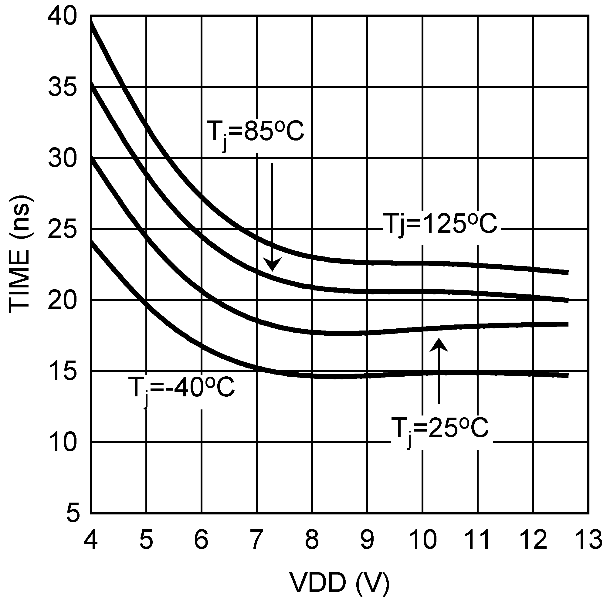 Figure 11. OUT Turnon Propagation Delay vs VDD
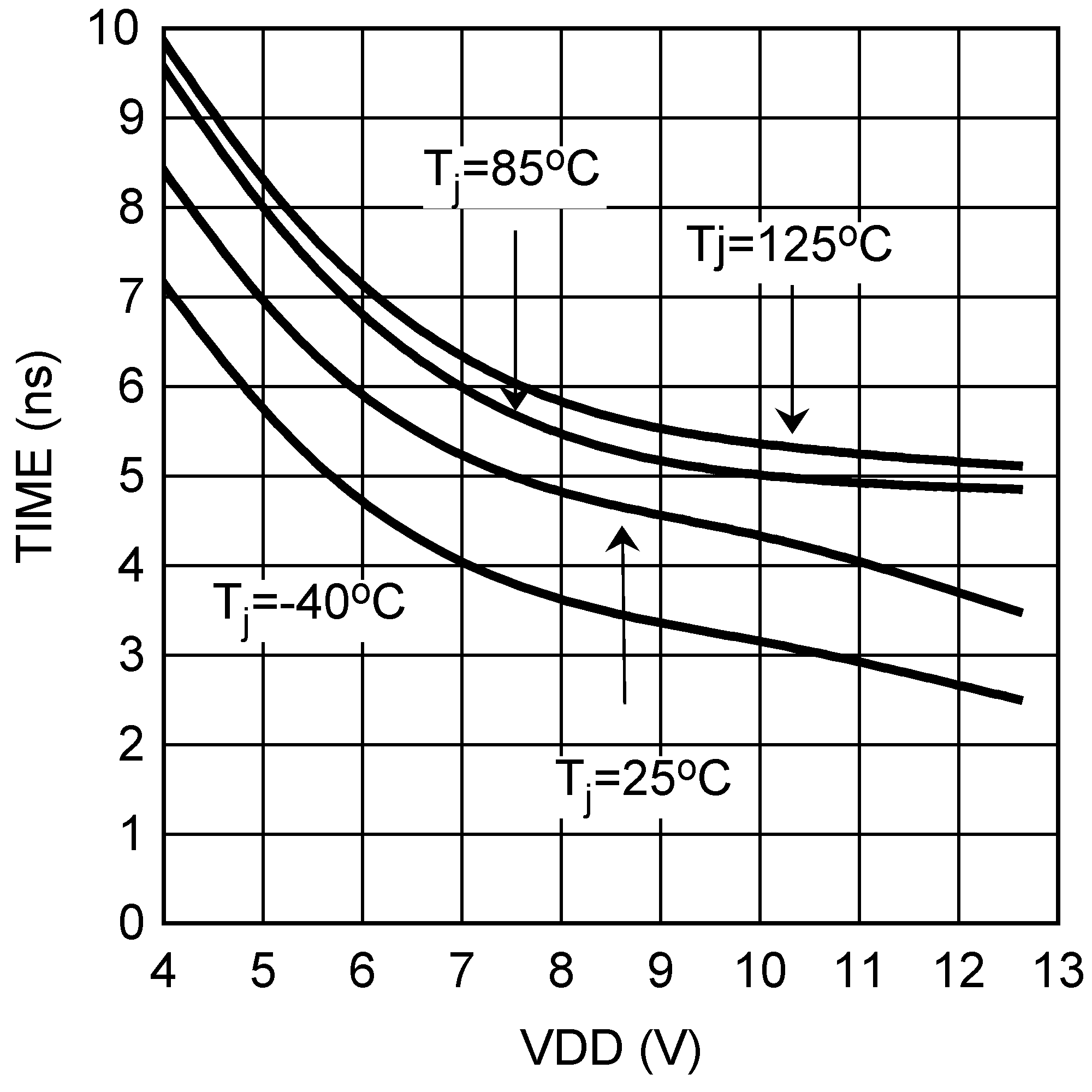 Figure 13. OUT Turnoff to PILOT Turnon Propagation Delay vs VDD
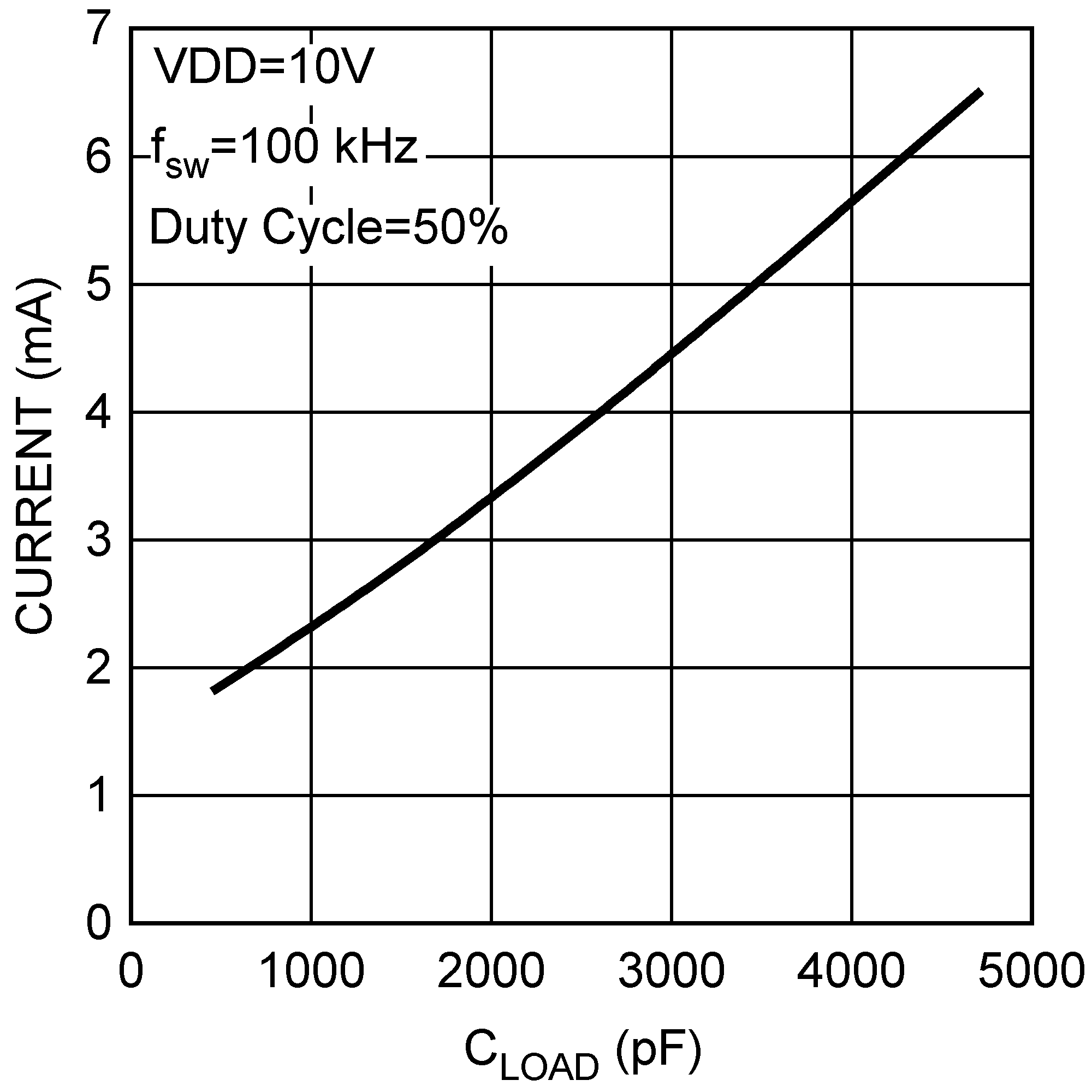 Figure 15. Supply Current vs OUT Capacitive Load
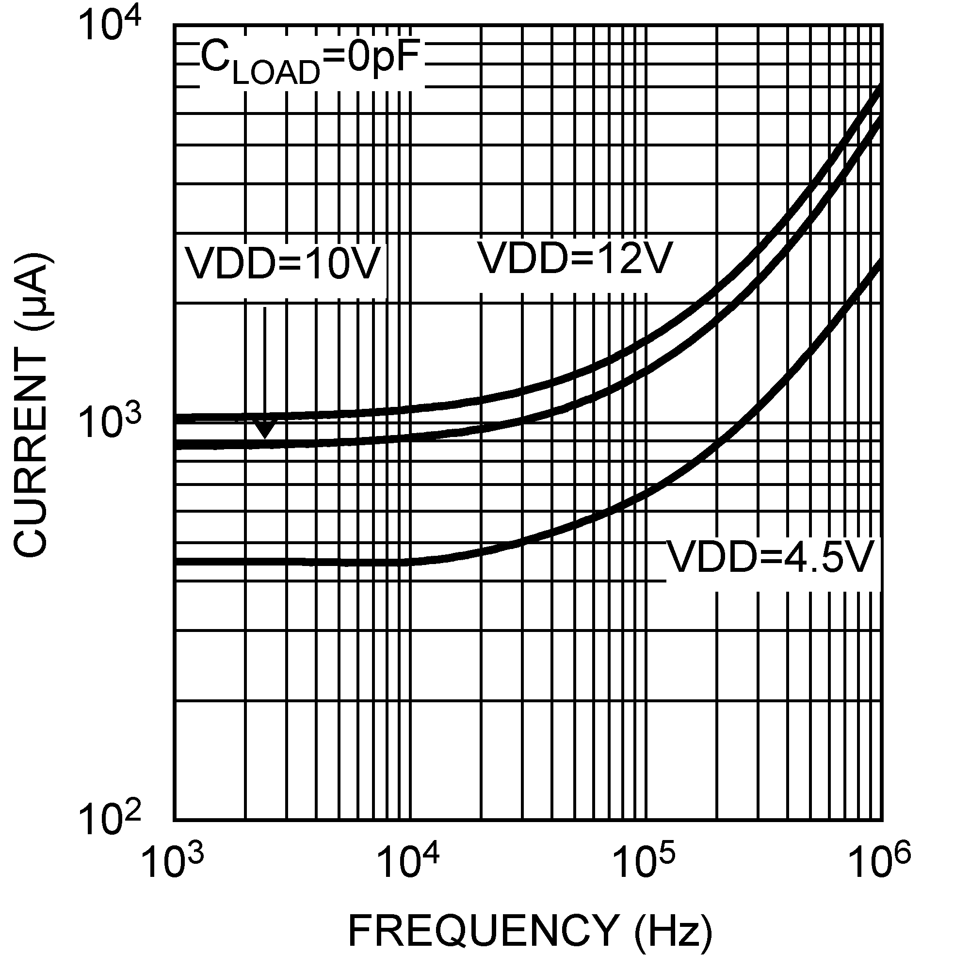 Figure 17. Supply Current vs Frequency
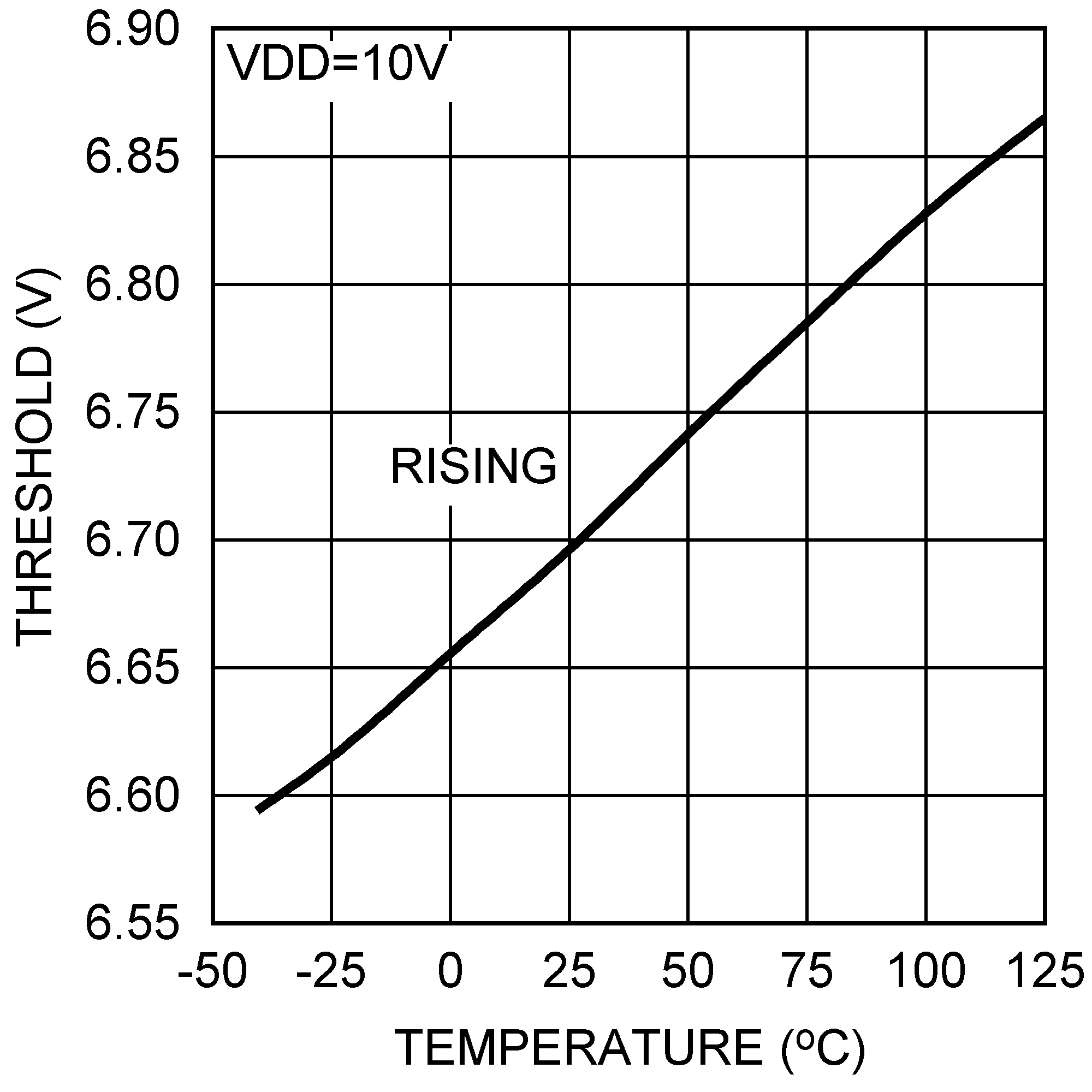 Figure 19. LM5134A Input Threshold vs Temperature
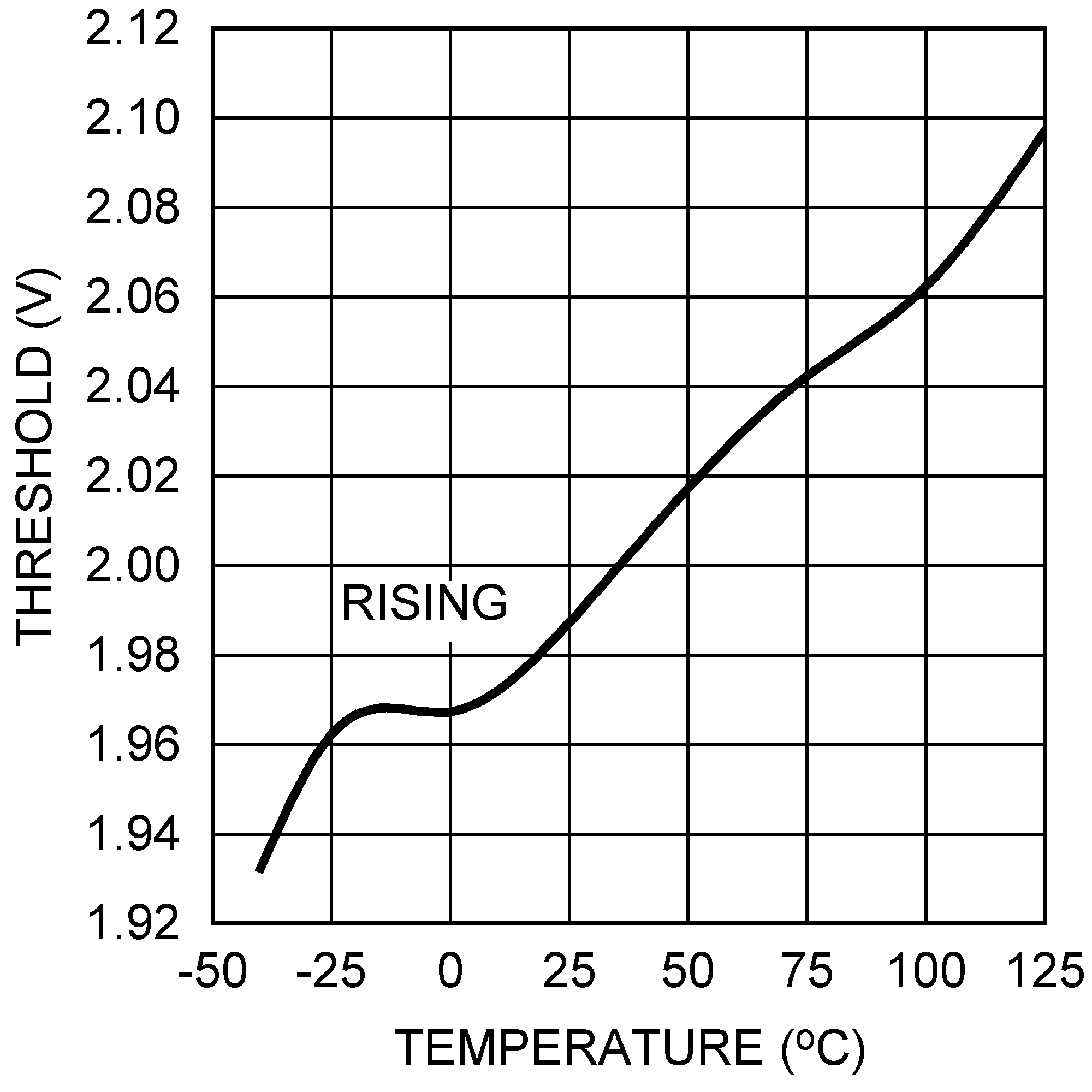 Figure 21. LM5134B Input Threshold vs Temperature
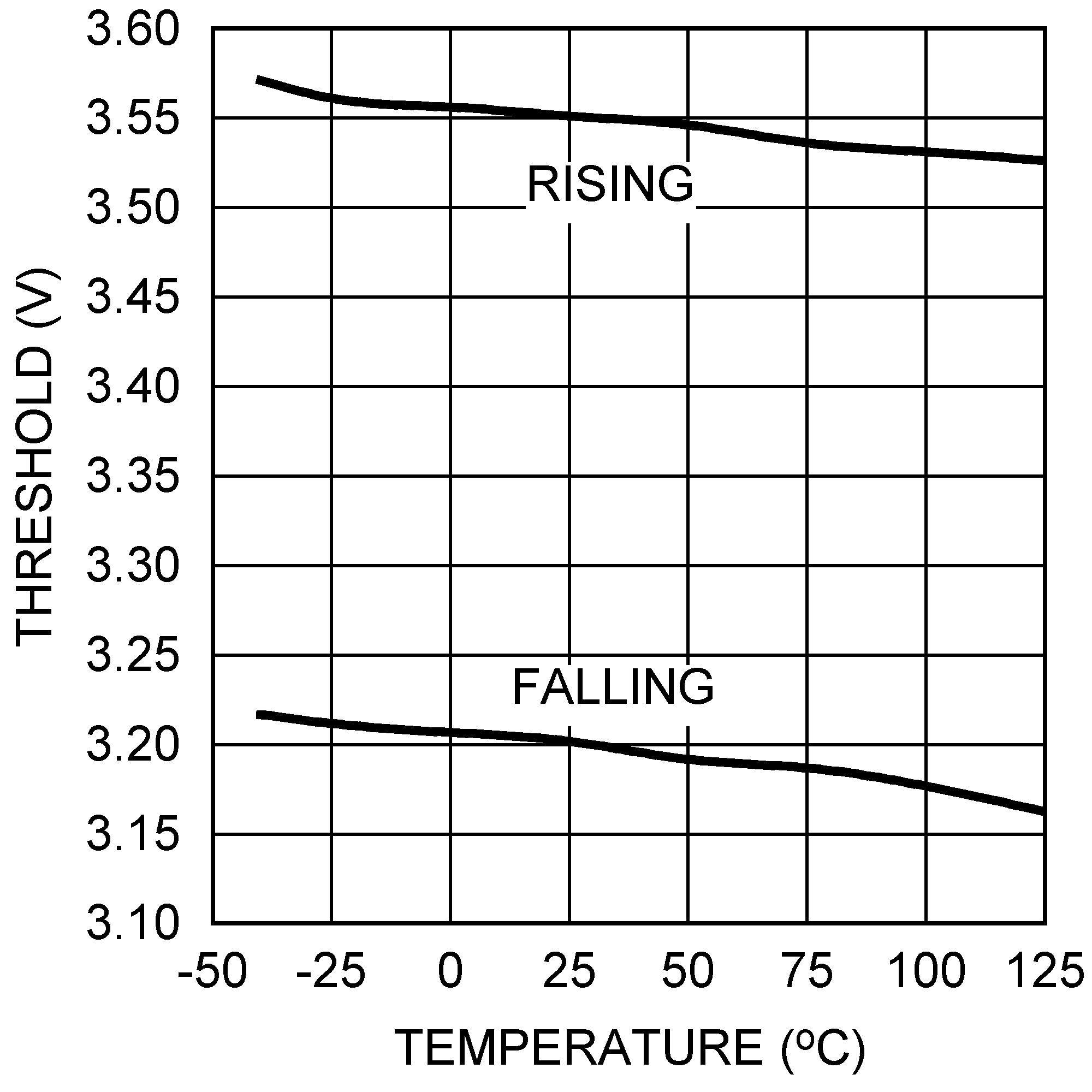 Figure 23. UVLO Threshold vs Temperature
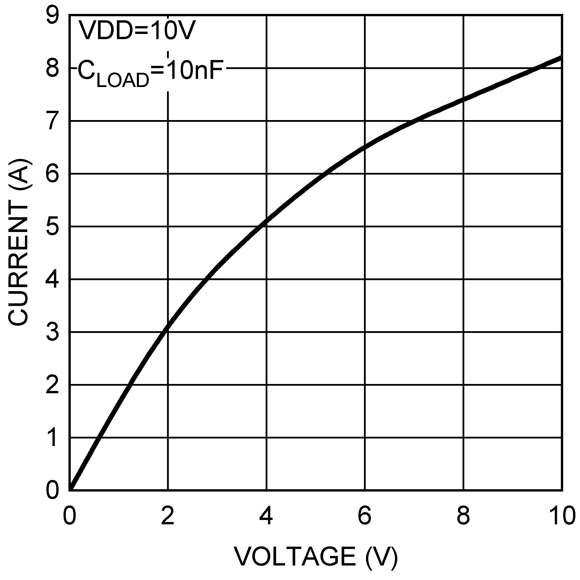 Figure 4. OUT Sink Current vs OUT Voltage
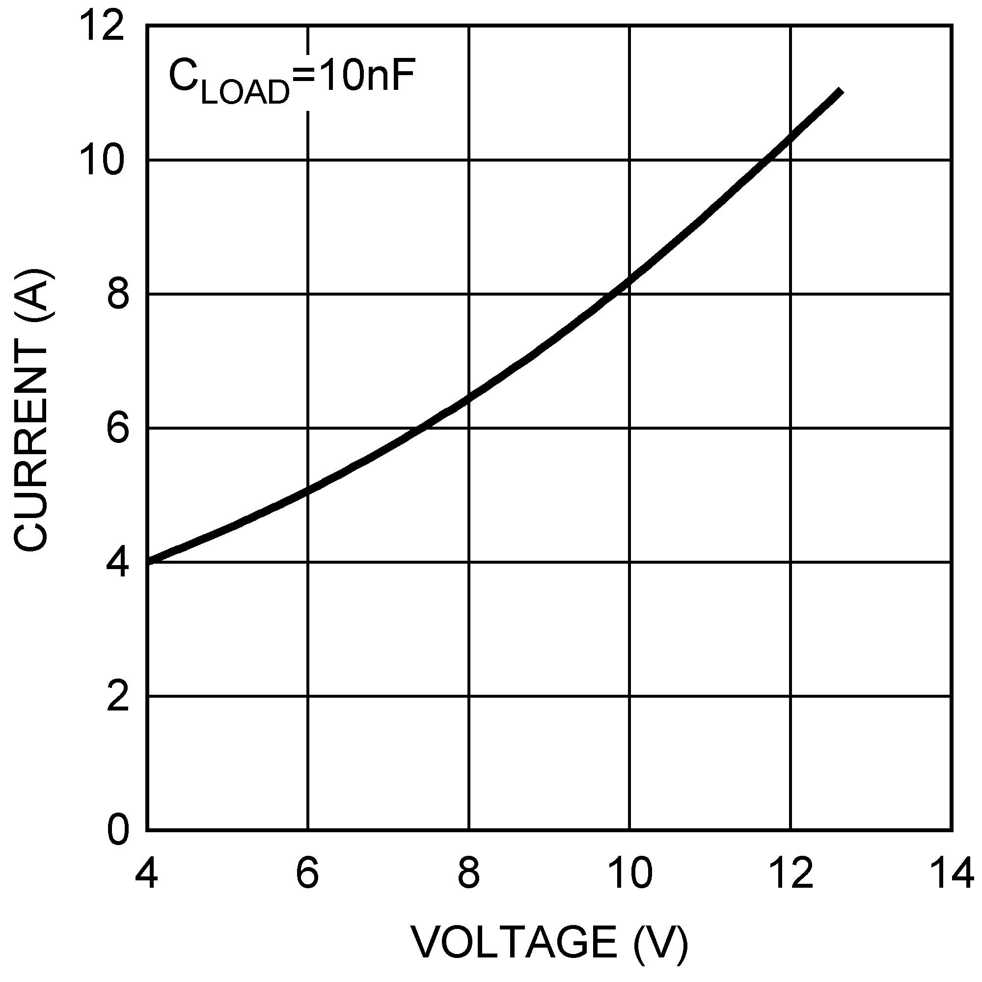 Figure 6. OUT Peak Sink Current vs VDD Voltage
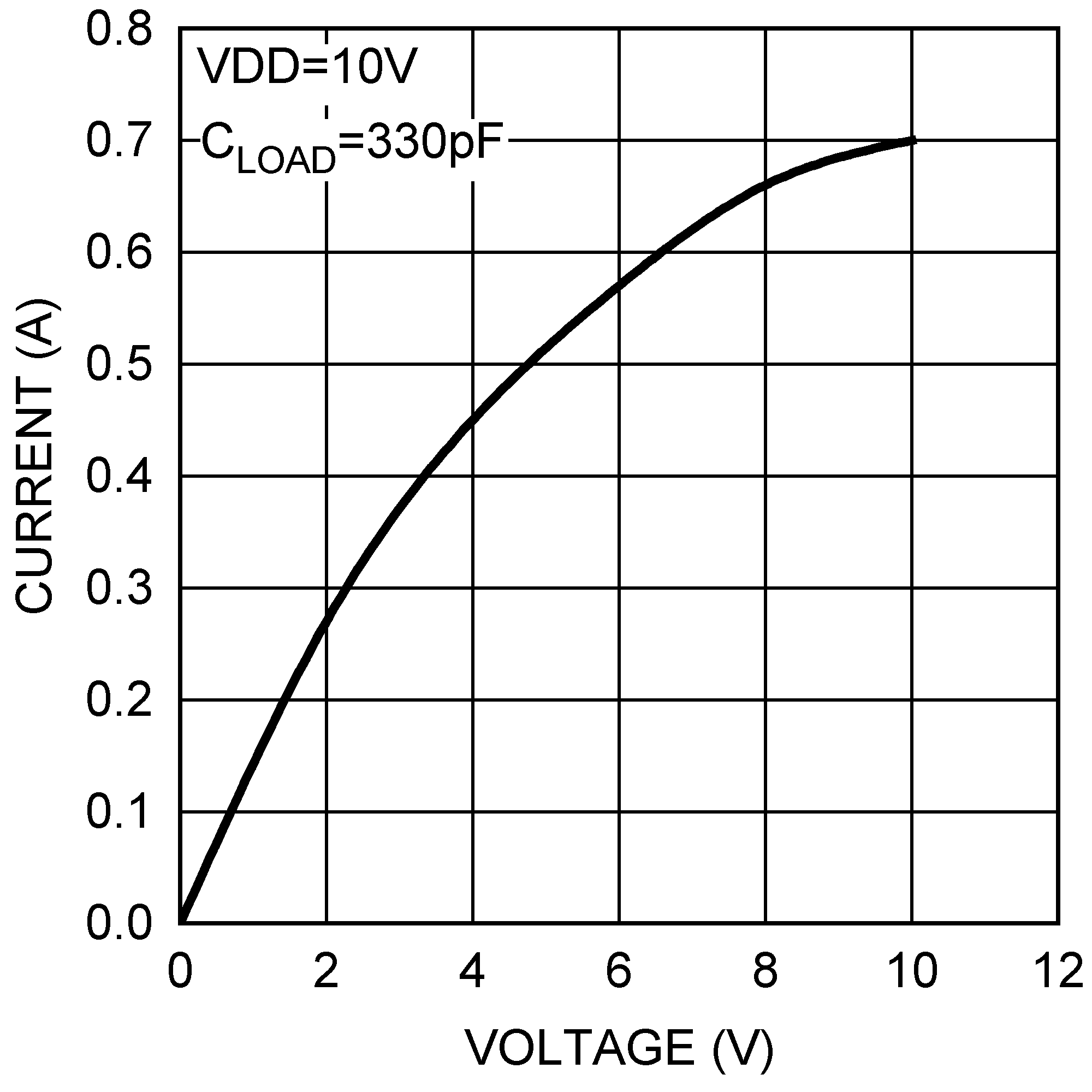 Figure 8. PILOT Sink Current vs PILOT Voltage
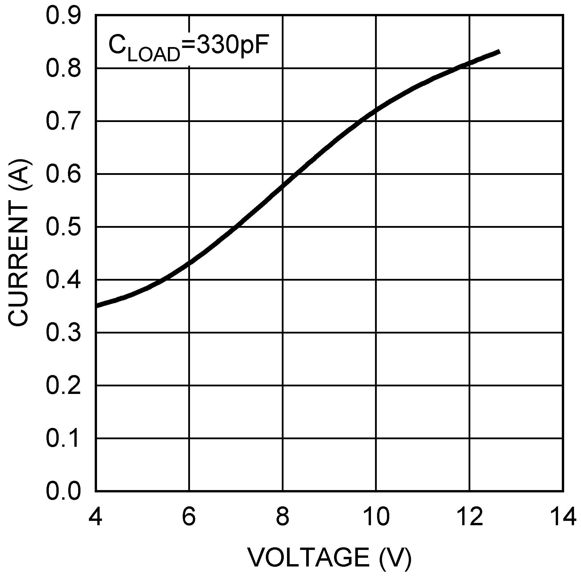 Figure 10. PILOT Peak Sink Current vs VDD Voltage
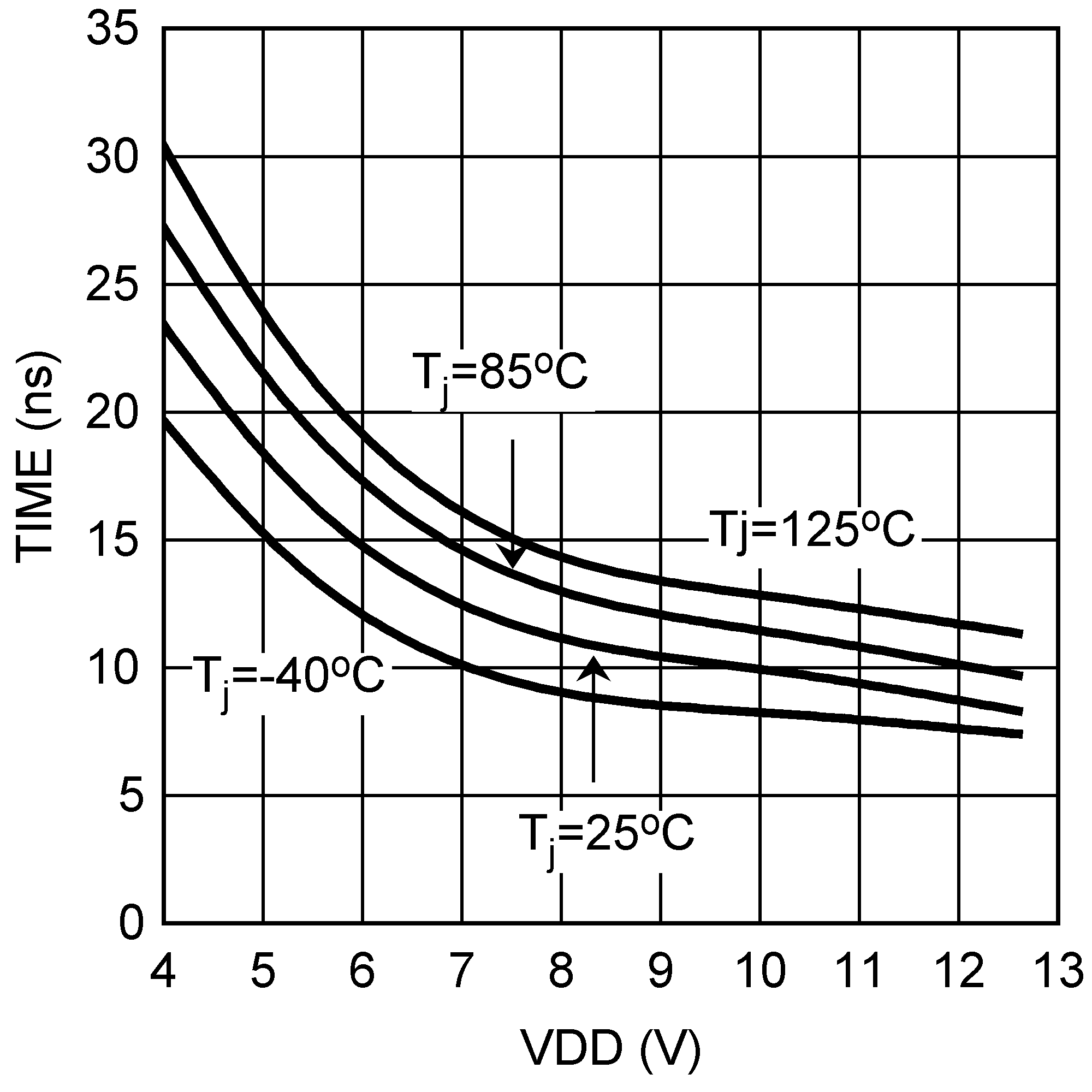 Figure 12. OUT Turnoff Propagation Delay vs VDD
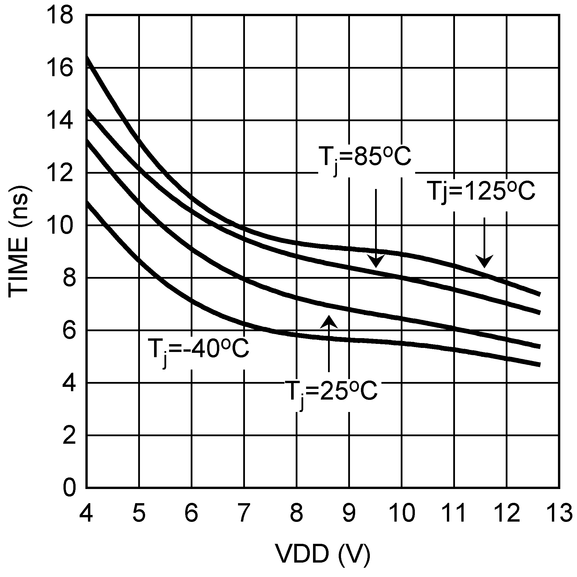 Figure 14. PILOT Turnoff to OUT Turnon Propagation Delay vs VDD
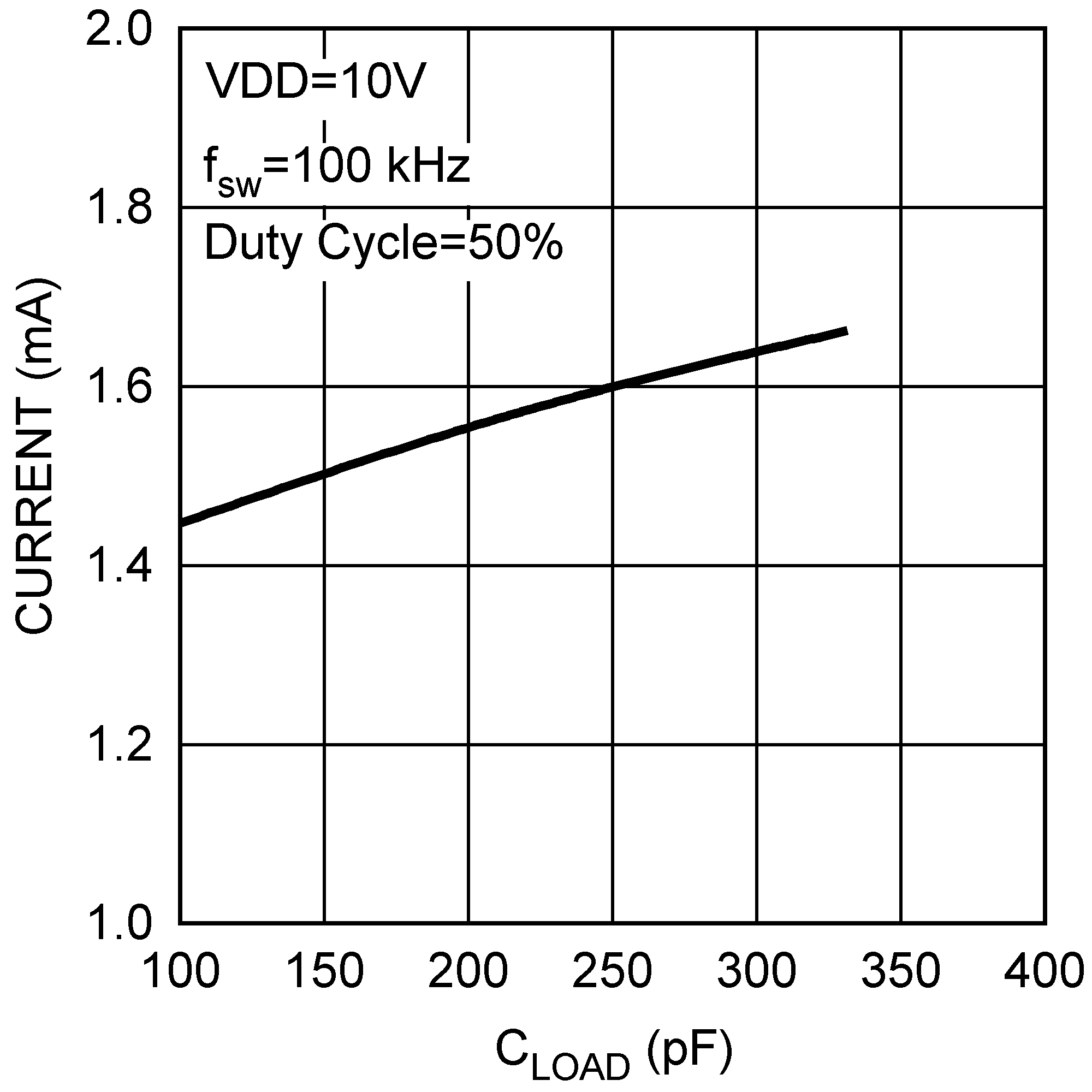 Figure 16. Supply Current vs PILOT Capacitive Load
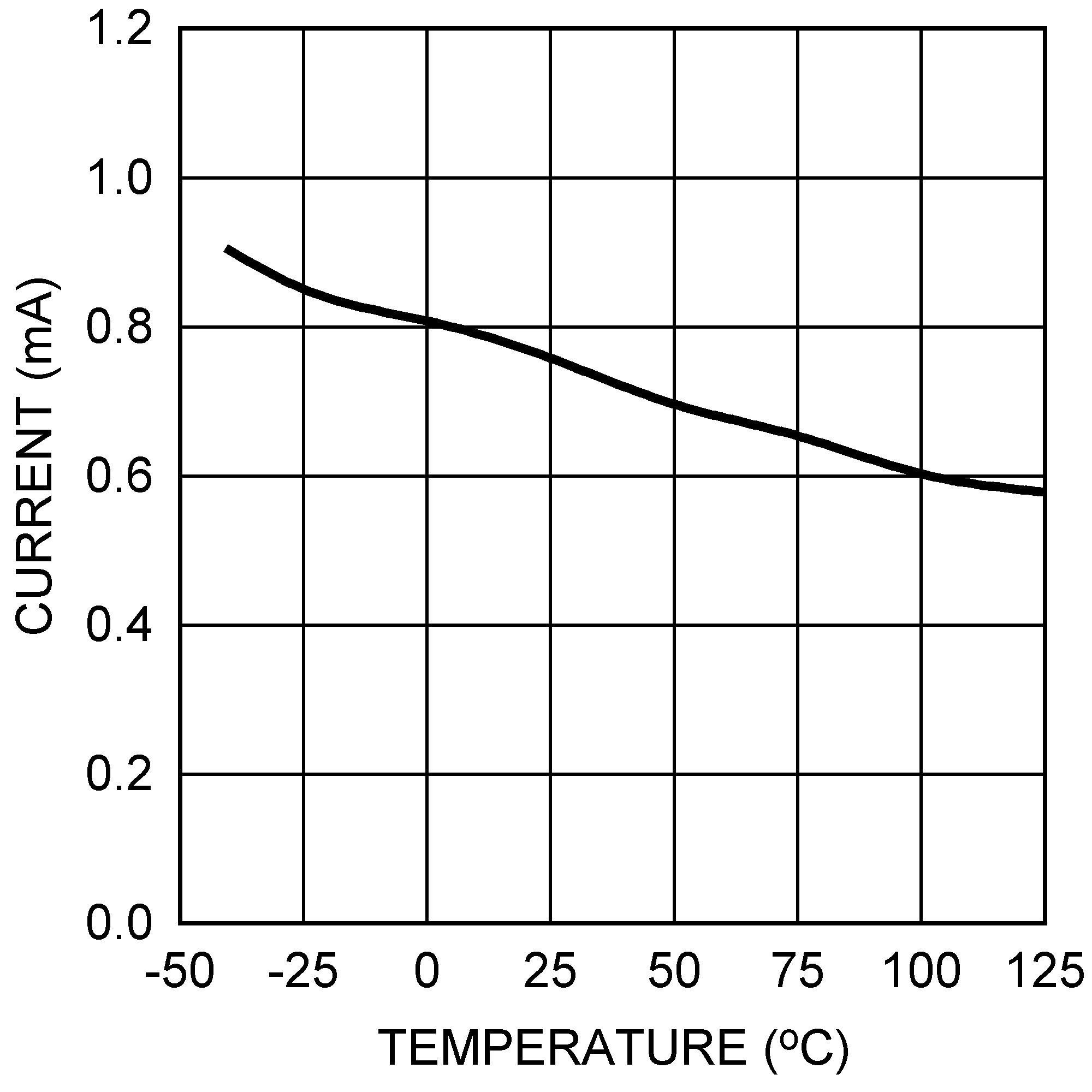 Figure 18. Quiescent Current vs Temperature
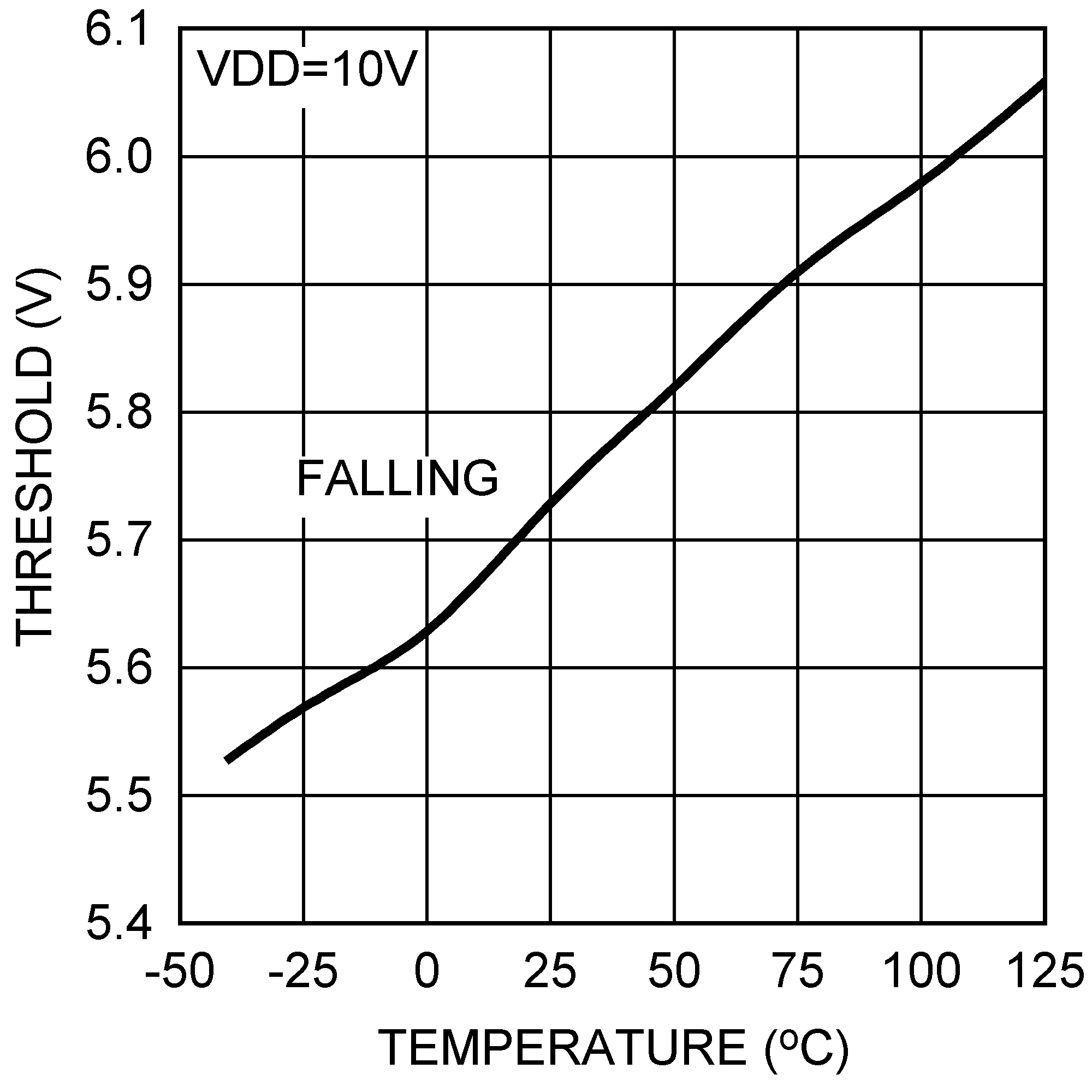 Figure 20. LM5134A Input Threshold vs Temperature
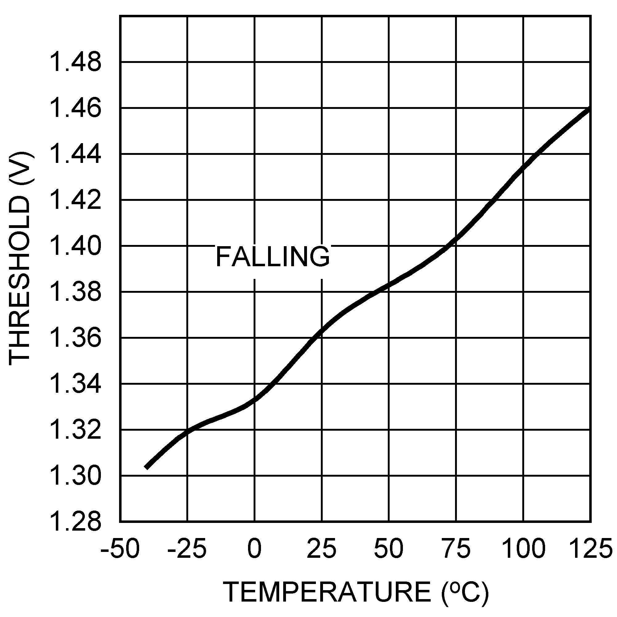 Figure 22. LM5134B Input Threshold vs Temperature