SNOSD08A September 2015 – October 2015 LM74670-Q1
PRODUCTION DATA.
- 1 Features
- 2 Applications
- 3 Description
- 4 Revision History
- 5 Pin Configuration and Functions
- 6 Specifications
- 7 Detailed Description
- 8 Application and Implementation
- 9 Power Supply Recommendations
- 10Layout
- 11Device and Documentation Support
- 12Mechanical, Packaging, and Orderable Information
- 14Mechanical, Packaging, and Orderable Information
Package Options
Mechanical Data (Package|Pins)
- DGK|8
Thermal pad, mechanical data (Package|Pins)
Orderable Information
1 Features
- AEC-Q100 Qualified With the Following Results:
- Device Temperature Grade 1: –40°C to +125°C Ambient Operating Temperature Range
- Exceeds HBM ESD Classification Level 2
- Device CDM ESD Classification Level C4B
- Peak Input AC Voltage: 42 V
- Zero IQ
- Charge Pump Gate Driver for external N-Channel MOSFET
- Low Forward-Voltage Drop and Less Power Dissipation Compared to Schottky Diode
- Capable of handling AC signal up to 300-Hz Frequency
2 Applications
- AC Rectifier
- Alternator
- Power Tools
- Reverse Polarity Protection
3 Description
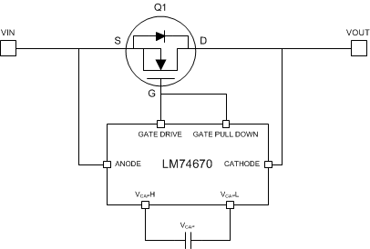
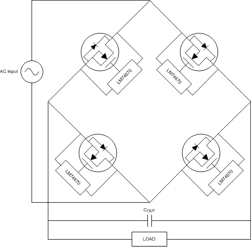
The LM74670-Q1 is a controller device that can be used with an N-Channel MOSFET in full or half bridge rectifier architectures for alternators. It is designed to drive an external MOSFET to emulate an ideal diode. A unique advantage of this scheme is that it is not ground referenced, thus it has zero IQ. The schottky diodes in full or half bridge rectifiers and alternators can be replaced with the LM74670-Q1 solution to avoid forward conduction diode losses and produce more efficient AC-DC converters.
The LM74670-Q1 controller provides a gate drive for external N-Channel MOSFET and a fast response internal comparator to pull-down the MOSFET Gate in the event of reverse polarity. This device can support an AC signal frequency up to 300Hz.
Device Information(1)
| PART NUMBER | PACKAGE | BODY SIZE (NOM) |
|---|---|---|
| LM74670-Q1 | VSSOP (8) | 3.00 mm × 5.00 mm |
- For all available packages, see the orderable addendum at the end of the data sheet.
Smart Diode Configuration

Smart Diode Full Bridge Rectifier Application
