LMP91000 Sensor AFE System: Configurable AFE Potentiostat for Low-Power Chemical-Sensing Applications
1 Features
- Typical Values, TA = 25°C
- Supply Voltage 2.7 V to 5.25 V
- Supply Current (Average Over Time) <10 µA
- Cell Conditioning Current Up to 10 mA
- Reference Electrode Bias Current (85°C) 900pA (max)
- Output Drive Current 750 µA
- Complete Potentiostat Circuit-to-Interface to Most Chemical Cells
- Programmable Cell Bias Voltage
- Low-Bias Voltage Drift
- Programmable TIA gain 2.75 kΩ to 350 kΩ
- Sink and Source Capability
- I2C Compatible Digital Interface
- Ambient Operating Temperature –40°C to 85°C
- Package 14-Pin WSON
- Supported by WEBENCH® Sensor AFE Designer
2 Applications
- Chemical Species Identification
- Amperometric Applications
- Electrochemical Blood Glucose Meter
3 Description
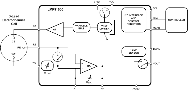
The LMP91000 is a programmable analog front-end (AFE) for use in micro-power electrochemical sensing applications. It provides a complete signal path solution between a sensor and a microcontroller that generates an output voltage proportional to the cell current. The LMP91000’s programmability enables it to support multiple electrochemical sensors such as 3-lead toxic gas sensors and 2-lead galvanic cell sensors with a single design as opposed to the multiple discrete solutions. The LMP91000 supports gas sensitivities over a range of 0.5 nA/ppm to 9500 nA/ppm. It also allows for an easy conversion of current ranges from 5 µA to 750 µA full scale.
The LMP91000’s adjustable cell bias and transimpedance amplifier (TIA) gain are programmable through the I2C interface. The I2C interface can also be used for sensor diagnostics. An integrated temperature sensor can be read by the user through the VOUT pin and used to provide additional signal correction in the µC or monitored to verify temperature conditions at the sensor.
The LMP91000 is optimized for micro-power applications and operates over a voltage range of 2.7 to 5.25 V. The total current consumption can be less than 10 μA. Further power savings are possible by switching off the TIA amplifier and shorting the reference electrode to the working electrode with an internal switch.
Device Information(1)
| PART NUMBER | PACKAGE | BODY SIZE (NOM) |
|---|---|---|
| LMP91000 | WSON (14) | 4.00 mm × 4.00 mm |
- For all available packages, see the orderable addendum at the end of the datasheet.
Simplified Application Schematic
4 Revision History
Changes from H Revision (March 2013) to I Revision
- Added ESD Ratings table, Feature Description section, Device Functional Modes, Application and Implementation section, Power Supply Recommendations section, Layout section, Device and Documentation Support section, and Mechanical, Packaging, and Orderable Information section Go
Changes from G Revision (March 2013) to H Revision
- Changed layout of National Data Sheet to TI formatGo
5 Pin Configuration and Functions
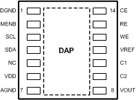
Pin Functions
| PIN | I/O | DESCRIPTION | |
|---|---|---|---|
| NAME | NO. | ||
| DGND | 1 | G | Connect to ground |
| MENB | 2 | I | Module Enable, Active-Low |
| SCL | 3 | I | Clock signal for I2C compatible interface |
| SDA | 4 | I/O | Data for I2C compatible interface |
| NC | 5 | N/A | Not Internally Connected |
| VDD | 6 | P | Supply Voltage |
| AGND | 7 | G | Ground |
| VOUT | 8 | O | Analog Output |
| C2 | 9 | N/A | External filter connector (Filter between C1 and C2) |
| C1 | 10 | N/A | External filter connector (Filter between C1 and C2) |
| VREF | 11 | I | Voltage Reference input |
| WE | 12 | I | Working Electrode. Output to drive the Working Electrode of the chemical sensor |
| RE | 13 | I | Reference Electrode. Input to drive Counter Electrode of the chemical sensor |
| CE | 14 | I | Counter Electrode. Output to drive Counter Electrode of the chemical sensor |
| DAP | — | N/C | Connect to AGND |
6 Specifications
6.1 Absolute Maximum Ratings
over operating free-air temperature (unless otherwise noted) (1)| MIN | MAX | UNIT | ||
|---|---|---|---|---|
| Voltage between any two pins | 6.0 | V | ||
| Current through VDD or VSS | 50 | mA | ||
| Current sunk and sourced by CE pin | 10 | mA | ||
| Current out of other pins(2) | 5 | mA | ||
| Junction Temperature (3) | 150 | °C | ||
| Storage temperature | –65 | 150 | °C | |
6.2 ESD Ratings
| VALUE | UNIT | |||
|---|---|---|---|---|
| V(ESD) | Electrostatic discharge | Human-body model (HBM), per ANSI/ESDA/JEDEC JS-001(1) | ±2000 | V |
| Charged-device model (CDM), per JEDEC specification JESD22-C101(2) | ±1000 | |||
6.3 Recommended Operating Conditions
| MIX | MAX | UNIT | |||
|---|---|---|---|---|---|
| Supply Voltage VS= (VDD - AGND) | 2.7 | 5.25 | V | ||
| Temperature Range(1) | –40 | 85 | °C | ||
6.4 Thermal Information
| THERMAL METRIC(1) | LMP91000 | UNIT | |
|---|---|---|---|
| WSON | |||
| 14 PINS | |||
| RθJA | Package Thermal Resistance | 44 | °C/W |
6.5 Electrical Characteristics
Unless otherwise specified, TA = 25°C, VS=(VDD – AGND), VS = 3.3 V and AGND = DGND = 0 V, VREF = 2.5 V, Internal Zero = 20% VREF.(1)| PARAMETER | TEST CONDITIONS | MIN(3) | TYP(2) | MAX(3) | UNIT | ||
|---|---|---|---|---|---|---|---|
| POWER SUPPLY SPECIFICATION | |||||||
| IS | Supply Current | 3-lead amperometric cell mode | µA | ||||
| MODECN = 0x03 | 10 | 13.5 | |||||
| –40 to 80°C (please verify that the degree is correct) | 15 | ||||||
| Standby mode | |||||||
| MODECN = 0x02 | 6.5 | 8 | |||||
| –40 to 80°C | 10 | ||||||
| Temperature Measurement mode with TIA OFF | |||||||
| MODECN = 0x06 | 11.4 | 13.5 | |||||
| –40 to 80°C | 15 | ||||||
| Temperature Measurement mode with TIA ON | |||||||
| MODECN = 0x07 | 14.9 | 18 | |||||
| –40 to 80°C | 20 | ||||||
| 2-lead ground-referred galvanic cell mode | |||||||
| VREF=1.5 V | 6.2 | ||||||
| MODECN = 0x01 | 8 | ||||||
| –40 to 80°C | 9 | ||||||
| Deep Sleep mode | |||||||
| MODECN = 0x00 | 0.6 | 0.85 | |||||
| –40 to 80°C | 1 | ||||||
| POTENTIOSTAT | |||||||
| Bias_RW | Bias Programming range (differential voltage between RE pin and WE pin) | Percentage of voltage referred to VREF or VDD | ±24% | ||||
| Bias Programming Resolution | First two smallest step | ±1 | |||||
| All other steps | ±2% | ||||||
| IRE | Input bias current at RE pin | VDD = 2.7 V | pA | ||||
| Internal Zero 50% VDD | –90 | 90 | |||||
| –40 to 80°C | –800 | 800 | |||||
| VDD = 5.25 V | |||||||
| Internal Zero 50% VDD | –90 | 90 | |||||
| –40 to 80°C | –900 | 900 | |||||
| ICE | Minimum operating current capability | sink | 750 | µA | |||
| source | 750 | ||||||
| Minimum charging capability(5) | sink | 10 | mA | ||||
| source | 10 | ||||||
| AOL_A1 | Open-loop voltage gain of control loop op amp (A1) | 300 mV ≤ VCE ≤ Vs-300 mV; | dB | ||||
| –750 µA ≤ICE ≤ 750 µA | |||||||
| –40 to 80°C | 104 | 120 | |||||
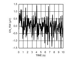
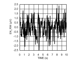
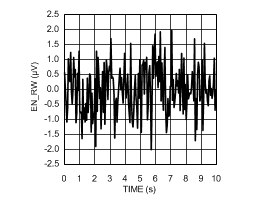
| en_RW | Low Frequency integrated noise between RE pin and WE pin | 0.1 Hz to 10 Hz, Zero Bias (6) |
3.4 | µVpp | |||
| 0.1 Hz to 10 Hz, with Bias (6)(7) |
5.1 | ||||||
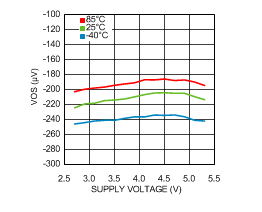
| VOS_RW | WE Voltage Offset referred to RE | BIAS polarity (8) –40 to 80°C |
0% VREF Internal Zero=20% VREF |
–550 | 550 | µV | |
| 0% VREF Internal Zero=50% VREF |
|||||||
| 0% VREF Internal Zero=67% VREF |
|||||||
| ±1% VREF | –575 | 575 | |||||
| ±2% VREF | –610 | 610 | |||||
| ±4% VREF | –750 | 750 | |||||
| ±6% VREF | –840 | 840 | |||||
| ±8% VREF | –930 | 930 | |||||
| ±10% VREF | –1090 | 1090 | |||||
| ±12% VREF | –1235 | 1235 | |||||
| ±14% VREF | –1430 | 1430 | |||||
| ±16% VREF | –1510 | 1510 | |||||
| ±18% VREF | –1575 | 1575 | |||||
| ±20% VREF | –1650 | 1650 | |||||
| ±22% VREF | –1700 | 1700 | |||||
| ±24% VREF | –1750 | 1750 | |||||
| TcVOS_RW | WE Voltage Offset Drift referred to RE from –40°C to 85°C (4) |
BIAS polarity (8) |
0% VREF Internal Zero=20% VREF |
–4 | 4 | µV/°C | |
| 0% VREF Internal Zero=50% VREF |
|||||||
| 0% VREF Internal Zero=67% VREF |
|||||||
| ±1% VREF | –4 | 4 | |||||
| ±2% VREF | –4 | 4 | |||||
| ±4% VREF | –5 | 5 | |||||
| ±6% VREF | –5 | 5 | |||||
| ±8% VREF | –5 | 5 | |||||
| ±10% VREF | –6 | 6 | |||||
| ±12% VREF | –6 | 6 | |||||
| ±14% VREF | –7 | 7 | |||||
| ±16% VREF | –7 | 7 | |||||
| ±18% VREF | –8 | 8 | |||||
| ±20% VREF | –8 | 8 | |||||
| ±22% VREF | –8 | 8 | |||||
| ±24% VREF | –8 | 8 | |||||
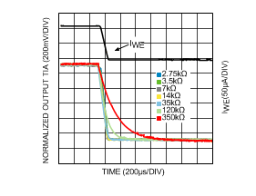
| TIA_GAIN | Transimpedance gain accuracy | 5% | |||||
| Linearity | ±0.05% | ||||||
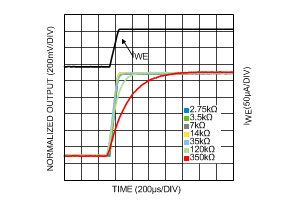
| Programmable TIA Gains | 7 programmable gain resistors | 2.75 3.5 7 14 35 120 350 |
kΩ | ||||
| Maximum external gain resistor | 350 | ||||||
| TIA_ZV | Internal zero voltage | 3 programmable percentages of VREF | 20% 50% 67% |
||||
| 3 programmable percentages of VDD | 20% 50% 67% |
||||||
| Internal zero voltage Accuracy | ±0.04% | ||||||
| RL | Programmable Load | 4 programmable resistive loads | 10 33 50 100 |
Ω | |||
| Load accuracy | 5% | ||||||
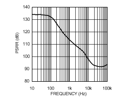
| PSRR | Power Supply Rejection Ratio at RE pin | 2.7 V ≤ VDD≤ 5.25 V | Internal zero 20% VREF | 80 | 110 | dB | |
| Internal zero 50% VREF | |||||||
| Internal zero 67% VREF | |||||||
| TEMPERATURE SENSOR SPECIFICATION (Refer to Table 1 in the Feature Description for details) | |||||||
| Temperature Error | TA= –40˚C to 85˚C | –3 | 3 | °C | |||
| Sensitivity | TA= –40˚C to 85˚C | -8.2 | mV/°C | ||||
| Power on time | 1.9 | ms | |||||
| EXTERNAL REFERENCE SPECIFICATION | |||||||
| VREF | External Voltage reference range | 1.5 | VDD | V | |||
| Input impedance | 10 | MΩ | |||||
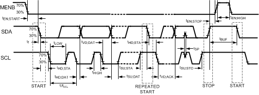
6.6 I2C Interface
Unless otherwise specified, TA = 25°C, VS = (VDD – AGND), 2.7 V <VS< 5.25 V and AGND = DGND = 0 V, VREF = 2.5 V.(1)| PARAMETER | TEST CONDITIONS | MIN (3) | TYP (2) | MAX(3) | UNIT | ||
|---|---|---|---|---|---|---|---|
| VIH | Input High Voltage |
–40 to 80°C |
0.7*VDD | V | |||
| VIL | Input Low Voltage |
–40 to 80°C |
0.3*VDD | V | |||
| VOL | Output Low Voltage | IOUT= 3 mA | 0.4 | V | |||
| Hysteresis (4) |
–40 to 80°C |
0.1*VDD | V | ||||
| CIN | Input Capacitance on all digital pins |
–40 to 80°C |
0.5 | pF | |||
6.7 Timing Requirements
Unless otherwise specified, TA = 25°C, VS= (VDD – AGND), VS= 3.3 V and AGND = DGND = 0 V, VREF = 2.5 V, Internal Zero= 20% VREF.(1)| MIN | TYP | MAX | UNIT | ||||
|---|---|---|---|---|---|---|---|
| fSCL | Clock Frequency | –40 to 80°C | 10 | 100 | kHz | ||
| tLOW | Clock Low Time | –40 to 80°C | 4.7 | µs | |||
| tHIGH | Clock High Time | –40 to 80°C | 4.0 | µs | |||
| tHD;STA | Data valid | After this period, the first clock pulse is generated | 4.0 | µs | |||
| tSU;STA | Set-up time for a repeated START condition | –40 to 80°C | 4.7 | µs | |||
| tHD;DAT | Data hold time(2)
|
–40 to 80°C | 0 | ns | |||
| tSU;DAT | Data Set-up time | –40 to 80°C | 250 | ns | |||
| tf | SDA fall time (3) | IL ≤ 3 mA; CL ≤ 400 pF –40 to 80°C |
250 | ns | |||
| tSU;STO | Set-up time for STOP condition | –40 to 80°C | 4.0 | µs | |||
| tBUF | Bus free time between a STOP and START condition | –40 to 80°C | 4.7 | µs | |||
| tVD;DAT | Data valid time | –40 to 80°C | 3.45 | µs | |||
| tVD;ACK | Data valid acknowledge time | –40 to 80°C | 3.45 | µs | |||
| tSP | Pulse width of spikes that must be suppressed by the input filter(3) | –40 to 80°C | 50 | ns | |||
| t_timeout | SCL and SDA Timeout | –40 to 80°C | 25 | 100 | ms | ||
| tEN;START | I2C Interface Enabling | –40 to 80°C | 600 | ns | |||
| tEN;STOP | I2C Interface Disabling | –40 to 80°C | 600 | ns | |||
| tEN;HIGH | Time between consecutive I2C interface enabling and disabling | –40 to 80°C | 600 | ns | |||
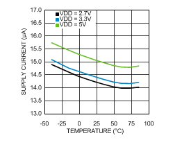
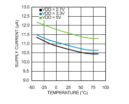
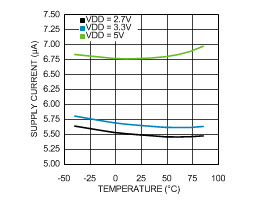
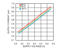
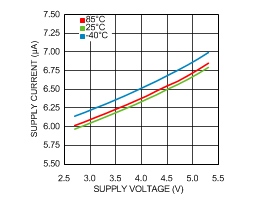
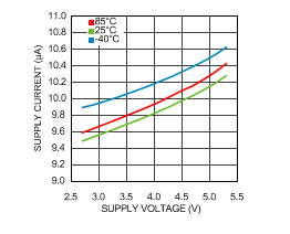
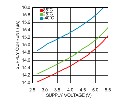
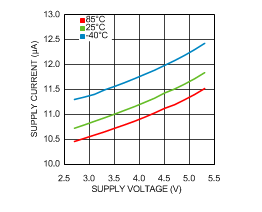
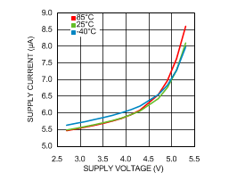
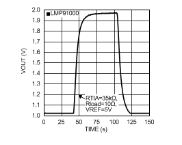
6.8 Typical Characteristics
Unless otherwise specified, TA = 25°C, VS= (VDD – AGND), 2.7V <VS< 5.25 V and AGND = DGND = 0 V, VREF = 2.5 V.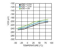
(Deep Sleep Mode)
(Standby Mode)
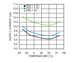
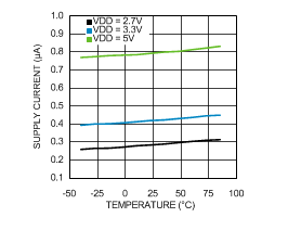
(3-Lead Amperometric Mode)
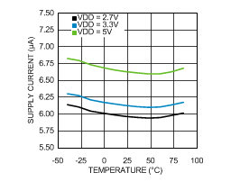
(Temp Measurement TIA On)
(Temp Measurement TIA Off)
(2-Lead Ground-Referred Amperometric Mode)
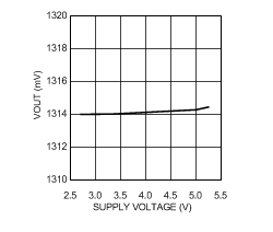
(Temperature = 30°C)
(Deep Sleep Mode)
(Standby Mode)
(3-Lead Amperometric Mode)
(Temp Measurement TIA On)
(Temp Measurement TIA Off)
(2-Lead Ground-Referred Amperometric Mode)
(CO Gas Sensor Connected to LMP91000)