LMX2531 High-Performance Frequency Synthesizer System With Integrated VCO
1 Features
- Multiple Frequency Options Available
- See Device Information Table
- Frequencies From: 553 MHz to 3132 MHz
- PLL Features
- Fractional-N Delta-Sigma Modulator Order Programmable up to Fourth Order
- FastLock/Cycle Slip Reduction with Timeout Counter
- Partially Integrated, Adjustable Loop Filter
- Very Low Phase Noise and Spurs
- VCO Features
- Integrated Tank Inductor
- Low Phase Noise
- Other Features
2 Applications
- Cellular Base Stations
- Wireless LANs
- Broadband Wireless Access
- Satellite Communications
- Wireless Radios
- Automotive
- CATV Equipment
- Instrumentation and Test Equipment
- RFID Readers
- Data Converter Clocking
3 Description
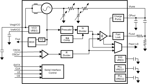
The LMX2531 is a low-power, high-performance frequency synthesizer system which includes a fully integrated delta-sigma PLL and VCO with fully integrated tank circuit. The third and fourth poles are also integrated and adjustable. Ultra-low noise and high-precision LDOs are integrated for the PLL and VCO, which yield higher supply-noise immunity and more consistent performance. When combined with a high-quality reference oscillator, the LMX2531 device generates very stable, low-noise local-oscillator signals for up and down conversion in wireless communication devices. The LMX2531 device is a monolithic integrated circuit, fabricated in an advanced BiCMOS process. Several different versions of this product accommodate different frequency bands.
Device Information(1)
| PART | LOW BAND | HIGH BAND |
|---|---|---|
| LMX2531LQ1146E | 553 — 592 MHz | 1106 — 1184 MHz |
| LMX2531LQ1226E | 592 — 634 MHz | 1184 — 1268 MHz |
| LMX2531LQ1312E | 634 — 680 MHz | 1268 — 1360 MHz |
| LMX2531LQ1415E | 680 — 735 MHz | 1360 — 1470 MHz |
| LMX2531LQ1500E | 749.5 — 755 MHz | 1499 — 1510 MHz |
| LMX2531LQ1515E | 725 — 790 MHz | 1450 — 1580 MHz |
| LMX2531LQ1570E | 765 — 818 MHz | 1530 — 1636 MHz |
| LMX2531LQ1650E | 795 — 850 MHz | 1590 — 1700 MHz |
| LMX2531LQ1700E | 831 — 885 MHz | 1662 — 1770 MHz |
| LMX2531LQ1742 | 880 — 933 MHz | 1760 — 1866 MHz |
| LMX2531LQ1778E | 863 — 920 MHz | 1726 — 1840 MHz |
| LMX2531LQ1910E | 917 — 1014 MHz | 1834 — 2028 MHz |
| LMX2531LQ2080E | 952 — 1137 MHz | 1904 — 2274 MHz |
| LMX2531LQ2265E | 1089 — 1200 MHz | 2178 — 2400 MHz |
| LMX2531LQ2570E | 1168 — 1395 MHz | 2336 — 2790 MHz |
| LMX2531LQ2820E | 1355 — 1462 MHz | 2710 — 2925 MHz |
| LMX2531LQ3010E | 1455 — 1566 MHz | 2910 — 3132 MHz |
- For all available packages, see the orderable addendum at the end of the datasheet.
Simplified Schematic
4 Revision History
Changes from R Revision (April 2013) to S Revision
- Added ESD Ratings table, Feature Description section, Device Functional Modes, Application and Implementation section, Power Supply Recommendations section, Layout section, Device and Documentation Support section, and Mechanical, Packaging, and Orderable Information sectionGo
Changes from Q Revision (February 2013) to R Revision
- Changed layout of National Data Sheet to TI formatGo
5 Pin Configuration and Functions

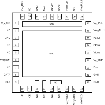
Pin Functions
| PIN | TYPE | DESCRIPTION | |
|---|---|---|---|
| NAME | NO. | ||
| CE | 11 | Input | Chip Enable Input. High impedance CMOS input. This pin must not exceed 2.75 V. When CE is brought high the LMX2531 is powered up corresponding to the internal power control bits. Although the part can be programmed when powered down, it is still necessary to reprogram the R0 register to get the part to re-lock. |
| CLK | 9 | Input | MICROWIRE clock input. High impedance CMOS input. This pin must not exceed 2.75 V. Data is clocked into the shift register on the rising edge. |
| CPout | 24 | Output | Charge pump output for PLL. For connection to Vtune through an external passive loop filter. |
| DATA | 8 | Input | MICROWIRE serial data input. High impedance CMOS input. This pin must not exceed 2.75 V. Data is clocked in MSB first. The last bits clocked in form the control or register select bits. |
| FLout | 25 | Output | An open drain NMOS output which is used for FastLock or a general purpose output. |
| Fout | 21 | Output | Buffered RF Output for the VCO. |
| Ftest/LD | 30 | Output | Multiplexed CMOS output. Typically used to monitor PLL lock condition. |
| GND | 3 | — | Ground |
| GND | 19 | — | Ground for the VCO circuitry. |
| GND | 20 | — | Ground for the VCO Output Buffer circuitry. |
| GND | 34 | — | Ground |
| LE | 10 | Input | MICROWIRE Latch Enable input. High impedance CMOS input. This pin must not exceed 2.75 V. Data stored in the shift register is loaded into the selected latch register when LE goes HIGH. |
| NC | 2, 4, 5, 7, 12, 13, 29, 35 | — | No Connect. |
| NC | 14, 15 | — | No Connect. Do NOT ground. This also includes the pad above these pins. |
| OSCin | 31 | Input | Oscillator input. |
| OSCin* | 32 | Input | Oscillator complimentary input. When a single ended source is used, then a bypass capacitor should be placed as close as possible to this pin and be connected to ground. |
| Test | 33 | Output | This pin is for test purposes and should be grounded for normal operation. |
| VccBUF | 22 | — | Power Supply for the VCO Buffer circuitry. Input may range from 2.8 — 3.2 V. Bypass capacitors should be placed as close as possible to this pin and ground. |
| VccDIG | 1 | — | Power Supply for digital LDO circuitry. Input may range from 2.8 — 3.2 V. Bypass capacitors should be placed as close as possible to this pin and ground. |
| VccPLL | 27 | — | Power Supply for the PLL. Input may range from 2.8 — 3.2 V. Bypass capacitors should be placed as close as possible to this pin and ground. |
| VccVCO | 16 | — | Power Supply for VCO regulator circuitry. Input may range from 2.8 — 3.2 V. Bypass capacitors should be placed as close as possible to this pin and ground. |
| VrefVCO | 18 | — | Internal reference voltage for VCO LDO. Not intended to drive an external load. Connect to ground with a capacitor. |
| VregBUF | 6 | — | Internally regulated voltage for the VCO buffer circuitry. Connect to ground with a capacitor. |
| VregDIG | 36 | — | Internally regulated voltage for LDO digital circuitry. |
| VregPLL1 | 26 | — | Internally regulated voltage for PLL charge pump. Not intended to drive an external load. Connect to ground with a capacitor. |
| VregPLL2 | 28 | — | Internally regulated voltage for RF digital circuitry. Not intended to drive an external load. Connect to ground with a capacitor. |
| VregVCO | 17 | — | Internally regulated voltage for VCO circuitry. Not intended to drive an external load. Connect to ground with a capacitor and some series resistance. |
| Vtune | 23 | Input | Tuning voltage input for the VCO. For connection to the CPout pin through an external passive loop filter. |