-
LP38798 800-mA Ultra-Low-Noise, High-PSRR LDO
- 1 Features
- 2 Applications
- 3 Description
- 4 Revision History
- 5 Pin Configuration and Functions
- 6 Specifications
- 7 Detailed Description
- 8 Application and Implementation
- 9 Power Supply Recommendations
- 10Layout
- 11Device and Documentation Support
- 12Mechanical, Packaging, and Orderable Information
- IMPORTANT NOTICE
Package Options
Mechanical Data (Package|Pins)
- DNT|12
Thermal pad, mechanical data (Package|Pins)
Orderable Information
LP38798 800-mA Ultra-Low-Noise, High-PSRR LDO
1 Features
- Wide Operating Input Voltage Range:
3 V to 20 V - Ultra-Low Output Noise: 5 µVRMS
(10 Hz to 100 kHz) - High PSRR: 90 dB at 10 kHz, 60 dB at 100 kHz
- ±1% Output Voltage Initial Accuracy (TJ = 25°C)
- Very Low Dropout: 200 mV (Typical) at 800 mA
- Stable with Ceramic or Tantalum Output Capacitors
- Excellent Line and Load Transient Response
- Current Limit and Overtemperature Protection
- Create a Custom Design Using the LP38798 With the WEBENCH® Power Designer
2 Applications
- RF Power Supplies: PLLs, VCOs, Mixers, LNAs
- Telecom Infrastructure
- Wireless Infrastructure
- Very Low-Noise Instrumentation
- Precision Power Supplies
- High-Speed, High-Precision Data Converters
3 Description
The LP38798-ADJ is a high-performance, low-noise LDO that can supply up to 800 mA output current. Designed to meet the requirements of sensitive RF/Analog circuitry, the LP38798-ADJ implements a novel linear topology on an advanced CMOS process to deliver ultra-low output noise and high PSRR at switching power supply frequencies. The LP38798SD-ADJ is stable with both ceramic and tantalum output capacitors and requires a minimum output capacitance of only 1 µF for stability.
The LP38798-ADJ can operate over a wide input voltage range (3 V to 20 V) making it well suited for many post-regulation applications.
Device Information(1)
| PART NUMBER | PACKAGE | BODY SIZE (NOM) |
|---|---|---|
| LP38798 | WSON (12) | 4.00 mm × 4.00 mm |
- For all available packages, see the orderable addendum at the end of the data sheet.
space
space
space
space
space
space
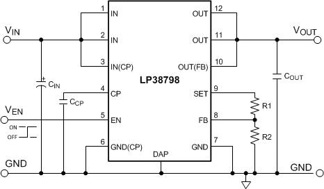
Simplified Schematic

4 Revision History
Changes from E Revision (August 2016) to F Revision
- Created Rev F toonly add WEBENCH links to data sheetGo
Changes from D Revision (June 2016) to E Revision
- Changed title of data sheet and updated list of Applications Go
- Changed first wording of first sentence of Description Go
Changes from C Revision (June2016) to D Revision
- Added 1.2 V row to Table 1 Go
- Changed "Value for R2 = 12.9 kΩ and 100 kΩ" to "R2 = 12.9 kΩ minimum to 100 kΩ maximum"Go
- Changed "value of 13.3 kΩ" to "value of 15 kΩ for R2"Go
- Changed "for R1 is" to "needed for R1 to provide an output voltage of 5 V is"Go
Changes from B Revision (December 2014) to C Revision
- Changed "linear regulator" to "LDO" on page 1; add top nav icon for reference designGo
- Changed Handling Ratings table to ESD Ratings table; move storage temperature to Abs Max table Go
- Added links for Community Resources Go
Changes from A Revision (May 2013) to B Revision
- Added Device Information and Handling Rating tables, Feature Description, Device Functional Modes, Application and Implementation, Power Supply Recommendations, Layout, Device and Documentation Support, and Mechanical, Packaging, and Orderable Information sections; updated Thermal Information; moved some curves to Application Curves sectionGo
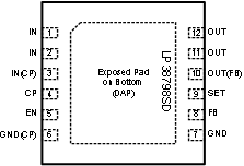
5 Pin Configuration and Functions

Pin Functions
| PIN | I/O | DESCRIPTION | |
|---|---|---|---|
| NUMBER | NAME | ||
| 1, 2 | IN | I | Device unregulated input voltage pins. Connect pins together at the package. |
| 3 | IN(CP) | I | Charge pump input voltage pin. Connect directly to pins 1 and 2 at the package. |
| 4 | CP | O | Charge pump output. See Charge Pump section in Application and Implementation for more information. |
| 5 | EN | I | Enable pin. This pin has an internal pullup to turn the LDO output on by default. A logic low level turns the LDO output Off, and reduce the operating current of the device. See Enable Input Operation section in Application and Implementation for more information. |
| 6 | GND(CP) | — | Device charge pump ground pin. |
| 7 | GND | — | Device analog ground pin. |
| 8 | FB | i | Feedback pin for programming the output voltage. |
| 9 | SET | I/O | Reference voltage output, and noise filter input. A feedback resistor divider network from this pin to FB and GND will set the output voltage of the device. |
| 10 | OUT(FB) | I | OUT buffer feedback input pin. Connect directly to pins 11 and 12 at the package. |
| 11, 12 | OUT | O | Device regulated output voltage pins. Connect pins together at the package. |
| Exposed Pad | DAP | — | The exposed die attach pad on the bottom of the package must be connected to a copper thermal pad on the PCB at ground potential. Connect to ground potential or leave floating. Do not connect to any potential other than the same ground potential seen at device pins 6 (GND(CP)) and 7 (GND). See Thermal Considerations section in Layout for more information. |