SNVS550E September 2009 – January 2017 LP5523
PRODUCTION DATA.
- 1 Features
- 2 Applications
- 3 Description
- 4 Revision History
- 5 Pin Configuration and Functions
-
6 Specifications
- 6.1 Absolute Maximum Ratings
- 6.2 ESD Ratings
- 6.3 Recommended Operating Conditions
- 6.4 Thermal Information
- 6.5 Electrical Characteristics
- 6.6 Charge Pump Electrical Characteristics
- 6.7 LED Driver Electrical Characteristics
- 6.8 LED Test Electrical Characteristics
- 6.9 Logic Interface Characteristics
- 6.10 Recommended External Clock Source Conditions
- 6.11 Serial Bus Timing Parameters (SDA, SCL)
- 6.12 Typical Characteristics
-
7 Detailed Description
- 7.1 Overview
- 7.2 Functional Block Diagram
- 7.3 Feature Description
- 7.4 Device Functional Modes
- 7.5 Programming
- 7.6 Register Maps
- 8 Application and Implementation
- 9 Power Supply Recommendations
- 10Layout
- 11Device and Documentation Support
- 12Mechanical, Packaging, and Orderable Information
Package Options
Mechanical Data (Package|Pins)
- YFQ|25
Thermal pad, mechanical data (Package|Pins)
Orderable Information
1 Features
- Three Independent Program Execution Engines, Nine Programmable Outputs with 25.5-mA Full-Scale Current, 8-Bit Current Setting Resolution, and 12-Bit PWM Control Resolution
- Adaptive High-Efficiency 1×/1.5× Fractional Charge Pump - Efficiency Up to 94%
- LED Drive Efficiency Up to 93%
- Charge Pump With Soft Start and Overcurrent and Short-Circuit Protection
- Built-in LED Test
- 200-nA Typical Standby Current
- Automatic Power-Save Mode
IVDD = 10 µA (Typical) - Two-Wire I2C-Compatible Control Interface
- Flexible Instruction Set
- Large SRAM Program Memory
- Small Application Circuit
- Source (High-Side) Drivers
- Architecture Supports Color Control
2 Applications
- Fun Lights and Indicator Lights
- LED Backlighting
- Haptic Feedback
- Programmable Current Source
3 Description
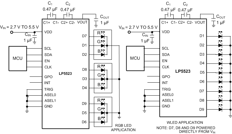
The LP5523 is a 9-channel LED driver designed to produce lighting effects for mobile devices. A high-efficiency charge pump enables LED driving over full Li-Ion battery voltage range. The device is equipped with an internal program memory, which allows operation without processor control.
The LP5523 maintains excellent efficiency over a wide operating range by autonomously selecting the best charge-pump gain based on LED forward voltage requirements. The LP5523 is able to automatically enter power-save mode when LED outputs are not active, thus lowering idle current consumption down to 10 µA (typical).
The LP5523 has an I2C-compatible control interface with four pin selectable addresses. The device has a flexible general purpose output (GPO), which can be used as a digital control pin for other devices. INT pin can be used to notify processor when a lighting sequence has ended (interrupt function). Also, the device has a trigger input interface, which allows synchronization, for example, between multiple LP5523 devices.
The device requires only four small, low-cost ceramic capacitors. The LP5523 is available in a tiny 25-pin DSBGA package (0.4-mm pitch).
Device Information(1)
| PART NUMBER | PACKAGE | BODY SIZE (NOM) |
|---|---|---|
| LP5523 | DSBGA (25) | 2.26 mm × 2.26 mm |
- For all available packages, see the orderable addendum at the end of the data sheet.
Typical Application
