-
OPA166x Low-Power, Low-Noise-and-Distortion, Bipolar-Input SoundPlus™ Audio Operational Amplifiers
Package Options
Refer to the PDF data sheet for device specific package drawings
Mechanical Data (Package|Pins)
- D|14
- PW|14
Thermal pad, mechanical data (Package|Pins)
Orderable Information
OPA166x Low-Power, Low-Noise-and-Distortion, Bipolar-Input SoundPlus™ Audio Operational Amplifiers
1 Features
- Low noise: 3.3nV/√Hz at 1kHz
- Low distortion: 0.00006% at 1kHz
- Low quiescent current:
1.5mA per channel - Slew rate: 17V/μs
- Wide gain bandwidth: 22MHz (G = +1)
- Unity gain stable
- Rail-to-rail output
- Wide supply range:
±1.5V to ±18V or 3V to 36V - Dual and quad versions available
- Small package sizes:
Dual: SOIC-8 and VSSOP-8
Quad: SOIC-14 and TSSOP-14
2 Applications
- USB and firewire audio systems
- Analog and digital mixers
- Portable recording systems
- Audio effects processors
- High-end A/V receivers
- High-end DVD and Blu-Ray™ players
- High-end car audio
3 Description
The dual OPA1662 and quad OPA1664 (OPA166x) series of bipolar-input SoundPlus™ audio operational amplifiers achieve a low 3.3nV/√Hz noise density with an ultra-low distortion of 0.00006% at 1kHz. The OPA166x series of op amps offer rail-to-rail output swing to within 600mV with 2kΩ load, which increases headroom and maximizes dynamic range. These devices also have a high output drive capability of ±30mA.
These devices operate over a very wide supply range of ±1.5V to ±18V, or 3V to 36V, on only 1.5mA of supply current per channel. The OPA166x op amps are unity-gain stable and provide excellent dynamic behavior over a wide range of load conditions.
These devices also feature completely independent circuitry for lowest crosstalk and freedom from interactions between channels, even when overdriven or overloaded.
The OPA166x are specified from –40°C to +85°C.
| PRODUCT | CHANNEL COUNT | PACKAGE(1) |
|---|---|---|
| OPA1662 | Dual | D (SOIC, 8) |
| DGK (VSSOP, 8) | ||
| OPA1664 | Quad | D (SOIC, 14) |
| PW (TSSOP, 14) |
4 Pin Configurations
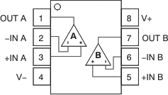 Figure 4-1 OPA1662: D and DGK Packages, SOIC-8 and
VSSOP-8 (Top View)
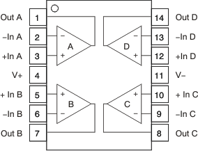 Figure 4-2 OPA1664: D and PW Packages, SOIC-14 and
TSSOP-14 (Top View)
Figure 4-2 OPA1664: D and PW Packages, SOIC-14 and
TSSOP-14 (Top View)5 Specifications
5.1 Absolute Maximum Ratings
| MIN | MAX | UNIT | ||
|---|---|---|---|---|
| VS | Supply voltage, VS = (V+) – (V–) | 40 | V | |
| Input voltage | (V–) – 0.5 | (V+) + 0.5 | V | |
| Input current (all pins except power-supply pins) | ±10 | mA | ||
| Output short-circuit(2) | Continuous | |||
| TA | Operating temperature | –55 | 125 | °C |
| TJ | Junction temperature | 150 | °C | |
| Tstg | Storage temperature | –65 | 150 | °C |
5.2 ESD Ratings
| VALUE | UNIT | |||
|---|---|---|---|---|
| V (ESD) | Electrostatic discharge | Human-body model (HBM), per ANSI/ESDA/JEDEC JS-001 (1) | 2000 | V |
| Charged-device model (CDM), per JEDEC specification JESD22-C101(2) | 1000 | |||
| Machine model (MM) | 200 | |||
5.3 Recommended Operating Conditions
| MIN | NOM | MAX | UNIT | |||
|---|---|---|---|---|---|---|
| VS | Supply voltage, (V+) – (V–) | ±1.5 | ±18 | V | ||
| TA | Ambient temperature | –40 | 85 | °C | ||
5.4 Thermal Information: OPA1662
| THERMAL METRIC(1) | OPA1662 | UNITS | ||
|---|---|---|---|---|
| D (SOIC) | DGK (VSSOP) | |||
| 8 PINS | 8 PINS | |||
| RθJA | Junction-to-ambient thermal resistance | 156.3 | 225.4 | °C/W |
| RθJCtop | Junction-to-case (top) thermal resistance | 85.5 | 78.8 | °C/W |
| RθJB | Junction-to-board thermal resistance | 64.9 | 110.5 | °C/W |
| ψJT | Junction-to-top characterization parameter | 33.8 | 14.6 | °C/W |
| ψJB | Junction-to-board characterization parameter | 64.3 | 108.5 | °C/W |
| RθJCbot | Junction-to-case (bottom) thermal resistance | N/A | N/A | °C/W |
5.5 Thermal Information: OPA1664
| THERMAL METRIC(1) | OPA1664 | UNITS | ||
|---|---|---|---|---|
| D (SOIC) | PW (TSSOP) | |||
| 14 PINS | 14 PINS | |||
| RθJA | Junction-to-ambient thermal resistance | 78.6 | 125.8 | °C/W |
| RθJCtop | Junction-to-case (top) thermal resistance | 37.0 | 45.2 | °C/W |
| RθJB | Junction-to-board thermal resistance | 24.9 | 57.5 | °C/W |
| ψJT | Junction-to-top characterization parameter | 9.7 | 5.5 | °C/W |
| ψJB | Junction-to-board characterization parameter | 24.6 | 56.7 | °C/W |
| RθJCbot | Junction-to-case (bottom) thermal resistance | N/A | N/A | °C/W |
5.6 Electrical Characteristics: VS = ±15V
| PARAMETER | TEST CONDITIONS | MIN | TYP | MAX | UNIT | ||
|---|---|---|---|---|---|---|---|
| AUDIO PERFORMANCE | |||||||
| THD+N | Total harmonic distortion + noise | G = +1, f = 1kHz, VO = 3VRMS | 0.00006 | % | |||
| –124 | dB | ||||||
| IMD | Intermodulation distortion | G = +1, VO = 3VRMS |
SMPTE/DIN two-tone, 4:1 (60Hz and 7kHz) |
0.00004 | % | ||
| –128 | dB | ||||||
| DIM 30 (3kHz square wave and 15kHz sine wave) |
0.00004 | % | |||||
| –128 | dB | ||||||
| CCIF
twin-tone (19kHz and 20kHz) |
0.00004 | % | |||||
| –128 | dB | ||||||
| FREQUENCY RESPONSE | |||||||
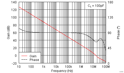
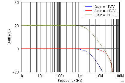
| GBW | Gain-bandwidth product | G = +1 | 22 | MHz | |||
| SR | Slew rate | G = –1 | 17 | V/μs | |||
| Full power bandwidth(1) | VO = 1VP | 2.7 | MHz | ||||
| Overload recovery time | G = –10 | 1 | μs | ||||
| Channel separation (dual and quad) | f = 1kHz | –120 | dB | ||||
| NOISE | |||||||
| en | Input voltage noise | f = 20Hz to 20kHz | 2.8 | μVPP | |||
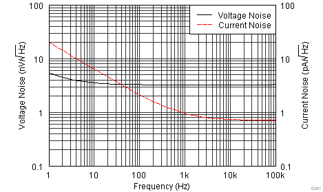
| Input voltage noise density | f = 1kHz | 3.3 | nV/√ Hz | ||||
| f = 100Hz | 5 | ||||||
| In | Input current noise density | f = 1kHz | 1 | pA/√ Hz | |||
| f = 100Hz | 2 | ||||||
| OFFSET VOLTAGE | |||||||
| VOS | Input offset voltage | VS = ±1.5V to ±18V | ±0.5 | ±1.5 | mV | ||
| VS = ±1.5V to ±18V, TA = –40°C to +85°C(2) | 2 | 8 | μV/°C | ||||
| PSRR | Power-supply rejection ratio | VS = ±1.5V to ±18V | 1 | 3 | μV/V | ||
| INPUT BIAS CURRENT | |||||||
| IB | Input bias current | VCM = 0V | 600 | 1200 | nA | ||
| IOS | Input offset current | VCM = 0V | ±25 | ±100 | nA | ||
| INPUT VOLTAGE | |||||||
| VCM | Common-mode voltage | (V–) + 0.5 | (V+) – 1 | V | |||
| CMRR | Common-mode rejection ratio | 106 | 114 | dB | |||
| INPUT IMPEDANCE | |||||||
| Differential | 170 || 2 | kΩ || pF | |||||
| Common-mode | 600 || 2.5 | MΩ || pF | |||||
| OPEN-LOOP GAIN | |||||||
| AOL | Open-loop voltage gain | (V–) + 0.6V ≤ VO ≤ (V+) – 0.6V, RL = 2kΩ | 106 | 114 | dB | ||
| OUTPUT | |||||||
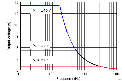
| VOUT | Output voltage | RL = 2kΩ | (V–) + 0.6 | (V+) – 0.6 | V | ||
| IOUT | Output current | See Typical Characteristics | mA | ||||
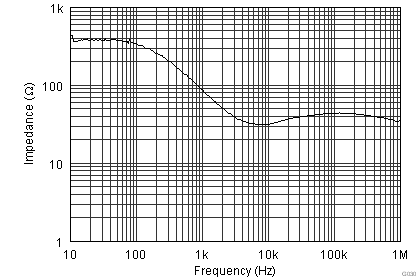
| ZO | Open-loop output impedance | See Typical Characteristics | Ω | ||||
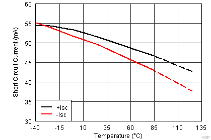
| ISC | Short-circuit current(3) | ±50 | mA | ||||
| CLOAD | Capacitive load drive | 200 | pF | ||||
| POWER SUPPLY | |||||||
| IQ | Quiescent current (per channel) |
IOUT = 0A | 1.5 | 1.8 | mA | ||
| TA = –40°C to +85°C(2) | 2 | ||||||
5.7 Electrical Characteristics: VS = 5V
| PARAMETER | TEST CONDITIONS | MIN | TYP | MAX | UNIT | ||
|---|---|---|---|---|---|---|---|
| AUDIO PERFORMANCE | |||||||
| THD+N | Total harmonic distortion + noise | G = +1, f = 1kHz, VO = 3VRMS | 0.0001 | % | |||
| –120 | dB | ||||||
| IMD | Intermodulation distortion | G = +1, VO = 3VRMS |
SMPTE/DIN two-tone, 4:1 (60Hz and 7kHz) |
0.00004 | % | ||
| –128 | dB | ||||||
| DIM 30 (3kHz square wave and 15kHz sine wave) |
0.00004 | % | |||||
| –128 | dB | ||||||
| CCIF
twin-tone (19kHz and 20kHz) |
0.00004 | % | |||||
| –128 | dB | ||||||
| FREQUENCY RESPONSE | |||||||
| GBW | Gain-bandwidth product | G = +1 | 20 | MHz | |||
| SR | Slew rate | G = –1 | 13 | V/μs | |||
| Full power bandwidth(1) | VO = 1VP | 2 | MHz | ||||
| Overload recovery time | G = –10 | 1 | μs | ||||
| Channel separation (dual and quad) | f = 1kHz | –120 | dB | ||||
| NOISE | |||||||
| en | Input voltage noise | f = 20Hz to 20kHz | 3.3 | μVPP | |||
| Input voltage noise density | f = 1kHz | 3.3 | nV/√ Hz | ||||
| f = 100Hz | 5 | ||||||
| In | Input current noise density | f = 1kHz | 1 | pA/√ Hz | |||
| f = 100Hz | 2 | ||||||
| OFFSET VOLTAGE | |||||||
| VOS | Input offset voltage | VS = ±1.5V to ±18V | ±0.5 | ±1.5 | mV | ||
| VS = ±1.5V to ±18V, TA = –40°C to +85°C(2) | 2 | 8 | μV/°C | ||||
| PSRR | Power-supply rejection ratio | VS = ±1.5V to ±18V | 1 | 3 | μV/V | ||
| INPUT BIAS CURRENT | |||||||
| IB | Input bias current | VCM = 0V | 600 | 1200 | nA | ||
| IOS | Input offset current | VCM = 0V | ±25 | ±100 | nA | ||
| INPUT VOLTAGE | |||||||
| VCM | Common-mode voltage | (V–) + 0.5 | (V+) – 1 | V | |||
| CMRR | Common-mode rejection ratio | 86 | 100 | dB | |||
| INPUT IMPEDANCE | |||||||
| Differential | 170 || 2 | kΩ || pF | |||||
| Common-mode | 600 || 2.5 | MΩ || pF | |||||
| OPEN-LOOP GAIN | |||||||
| AOL | Open-loop voltage gain | (V–) + 0.6V ≤ VO ≤ (V+) – 0.6V, RL = 2kΩ | 90 | 100 | dB | ||
| OUTPUT | |||||||
| VOUT | Output voltage | RL = 2kΩ | (V–) + 0.6 | (V+) – 0.6 | V | ||
| IOUT | Output current | See Typical Characteristics | mA | ||||
| ZO | Open-loop output impedance | See Typical Characteristics | Ω | ||||
| ISC | Short-circuit current(3) | ±40 | mA | ||||
| CLOAD | Capacitive load drive | 200 | pF | ||||
| POWER SUPPLY | |||||||
| IQ | Quiescent current (per channel) |
IOUT = 0A | 1.4 | 1.7 | mA | ||
| TA = –40°C to +85°C(2) | 2 | ||||||
5.8 Typical Characteristics
at TA = +25°C, VS = ±15V, and RL = 2kΩ (unless otherwise noted)

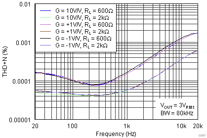
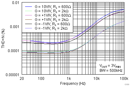
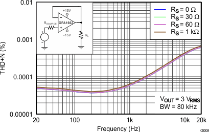

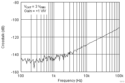


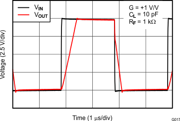
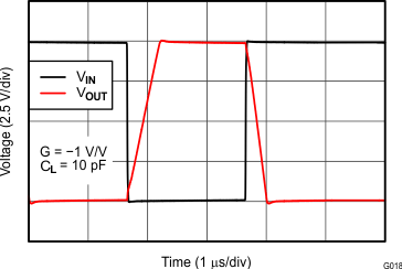


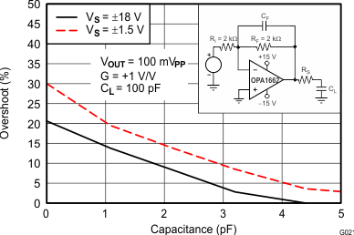
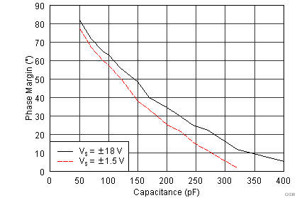




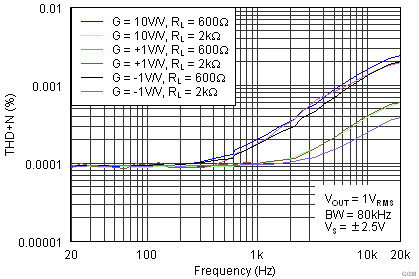
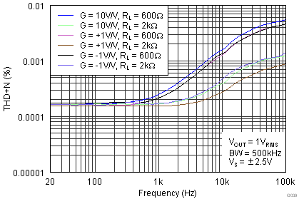
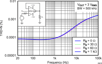


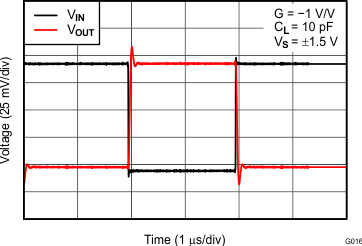
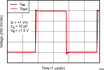

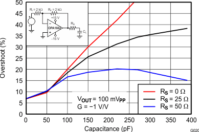
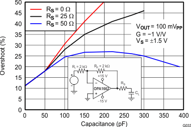
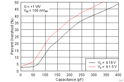
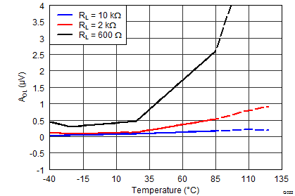
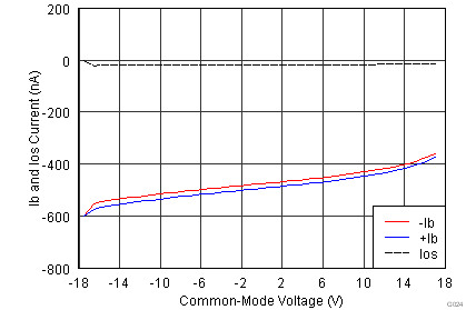
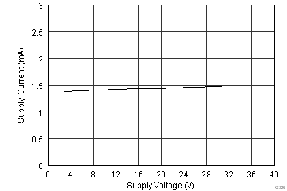

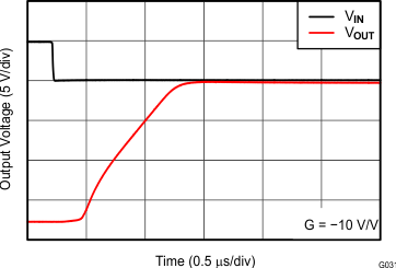

6 Application and Implementation
Information in the following applications sections is not part of the TI component specification, and TI does not warrant its accuracy or completeness. TI’s customers are responsible for determining suitability of components for their purposes, as well as validating and testing their design implementation to confirm system functionality.