-
OPAx316 10-MHz, Low-Power, Low-Noise, RRIO, 1.8-V CMOS Operational Amplifier
- 1 Features
- 2 Applications
- 3 Description
- 4 Revision History
- 5 Pin Configuration and Functions
- 6 Specifications
- 7 Detailed Description
- 8 Application and Implementation
- 9 Power Supply Recommendations
- 10Layout
- 11Device and Documentation Support
- 12Mechanical, Packaging, and Orderable Information
- 11Mechanical, Packaging, and Orderable Information
- IMPORTANT NOTICE
Package Options
Mechanical Data (Package|Pins)
Thermal pad, mechanical data (Package|Pins)
Orderable Information
OPAx316 10-MHz, Low-Power, Low-Noise, RRIO, 1.8-V CMOS Operational Amplifier
1 Features
2 Applications
- Battery-Powered Instruments:
- Consumer, Industrial, Medical
- Notebooks, Portable Media Players
- Sensor Signal Conditioning
- Automotive Applications
- Barcode Scanners
- Active Filters
- Audio
3 Description
The OPAx316 family of single, dual, and quad operational amplifiers represents a new generation of general-purpose, low-power operational amplifiers. Featuring rail-to-rail input and output swings, low quiescent current (400 μA/ch typical) combined with a wide bandwidth of 10 MHz and very-low noise
(11 nV/√Hz at 1 kHz) makes this family attractive for a variety of applications that require a good balance between cost and performance. The low input bias current supports those operational amplifiers to be used in applications with MΩ source impedances.
The robust design of the OPAx316 provide ease-of-use to the circuit designer—a unity-gain stable, integrated RFI-EMI rejection filter, no phase reversal in overdrive condition, and high electrostatic discharge (ESD) protection (4-kV HBM).
These devices are optimized for low-voltage operation as low as 1.8 V (±0.9 V) and up to 5.5 V (±2.75 V). This latest addition of low-voltage CMOS operational amplifiers, in conjunction with the OPAx313 and OPAx314 provide a family of bandwidth, noise, and power options to meet the needs of a wide variety of applications.
Device Information(1)
- For all available packages, see the orderable addendum at the end of the data sheet.
SPACE
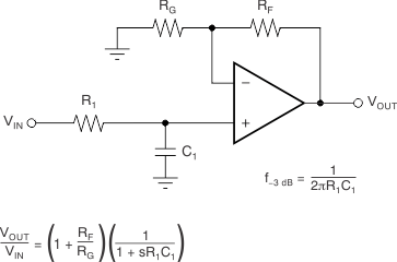
Single-Pole, Low-Pass Filter
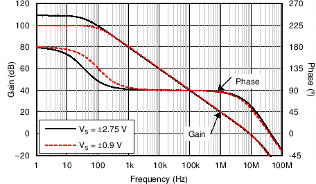
Low-Supply Current (400 µA/ch) for 10-MHz Bandwidth
4 Revision History
Changes from E Revision (May 2016) to F Revision
- Added SOIC (14) / OPA4316 body size information to Device Information table Go
- Added D package to PW package pinout drawing Go
- Added D (SOIC) thermal information to Thermal Information: OPA4316 table Go
Changes from D Revision (December 2014) to E Revision
- Added new "RUG" packageGo
Changes from C Revision (October 2014) to D Revision
- Added Shutdown section to Electrical Characteristics table Go
- Added Related Documentation section Go
Changes from B Revision (August 2014) to C Revision
- Updated devices and packages in Device Information table Go
- Added thermal information for OPA2316S and OPA4316Go
Changes from A Revision (April 2014) to B Revision
- Added OPA2316 to the Device Information tableGo
- Added thermal information for OPA2316 Go
- Added channel separation to Electrical Characteristics Go
- Added GBP instead of UGB in the Electrical Characteristics Go
- Added Channel Separation vs Frequency plotGo
Changes from * Revision (April 2014) to A Revision
- Changed status from preview to production Go
5 Pin Configuration and Functions
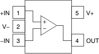
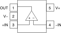
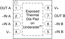
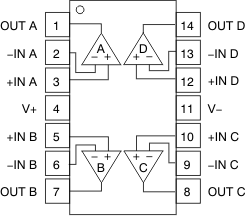
NOINDENT:
Pitch: 0.5 mm.NOINDENT:
Connect thermal pad to V–. Pad size: 2.00 mm × 1.20 mm.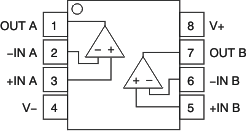
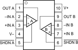
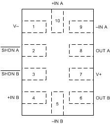
Pin Functions
| PIN | DESCRIPTION | |||||||
|---|---|---|---|---|---|---|---|---|
| NAME | OPA316 | OPA2316 | OPA2316S | OPA4316 | ||||
| DBV | DCK | D, DGK, DRG | DGS | RUG | PW | D | ||
| +IN | 3 | 1 | — | — | — | — | — | Noninverting input |
| +IN A | — | — | 3 | 3 | 10 | 3 | 3 | Noninverting input |
| +IN B | — | — | 5 | 7 | 4 | 5 | 5 | Noninverting input |
| +IN C | — | — | — | — | — | 10 | 10 | Noninverting input |
| +IN D | — | — | — | — | — | 12 | 12 | Noninverting input |
| –IN | 4 | 3 | — | — | — | — | — | Inverting input |
| –IN A | — | — | 2 | 2 | 9 | 2 | 2 | Inverting input |
| –IN B | — | — | 6 | 8 | 5 | 6 | 6 | Inverting input |
| –IN C | — | — | — | — | — | 9 | 9 | Inverting input |
| –IN D | — | — | — | — | — | 13 | 13 | Inverting input |
| OUT | 1 | 4 | — | — | — | — | — | Output |
| OUT A | — | — | 1 | 1 | 8 | 1 | 1 | Output |
| OUT B | — | — | 7 | 9 | 6 | 7 | 7 | Output |
| OUT C | — | — | — | — | — | 8 | 8 | Output |
| OUT D | — | — | — | — | — | 14 | 14 | Output |
| SHDN A | — | — | — | 5 | 2 | — | — | Shutdown (logic low), enable (logic high) |
| SHDN B | — | — | — | 6 | 3 | — | — | Shutdown (logic low), enable (logic high) |
| V+ | 5 | 5 | 8 | 10 | 7 | 4 | 4 | Positive supply |
| V– | 2 | 2 | 4 | 4 | 1 | 11 | 11 | Negative supply or ground (for single-supply operation) |
