-
SN74LVC2G00 Dual 2-Input Positive-NAND Gate
- 1 Features
- 2 Applications
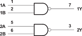
- 3 Description
- 4 Simplified Schematic
- 5 Revision History
- 6 Pin Configuration and Functions
- 7 Specifications
- 8 Parameter Measurement Information
- 9 Detailed Description
- 10Application and Implementation
- 11Power Supply Recommendations
- 12Layout
- 13Device and Documentation Support
- 14Mechanical, Packaging, and Orderable Information
- IMPORTANT NOTICE
Package Options
Refer to the PDF data sheet for device specific package drawings
Mechanical Data (Package|Pins)
- DCU|8
- YZP|8
- DCT|8
Thermal pad, mechanical data (Package|Pins)
Orderable Information
DATA SHEET
SN74LVC2G00 Dual 2-Input Positive-NAND Gate
1 Features
- Available in the Texas Instruments
NanoFree™ Package - Supports 5-V VCC Operation
- Inputs Accept Voltages to 5.5 V
- Max tpd of 4.3 ns at 3.3 V
- Low Power Consumption, 10-μA Max ICC
- ±24-mA Output Drive at 3.3 V
- Typical VOLP (Output Ground Bounce)
< 0.8 V at VCC = 3.3 V, TA = 25°C - Typical VOHV (Output VOH Undershoot)
> 2 V at VCC = 3.3 V, TA = 25°C - Ioff Supports Live Insertion, Partial Power
Down Mode, and Back Drive Protection - Latch-Up Performance Exceeds 100 mA
Per JESD 78, Class II - ESD Protection Exceeds JESD 22
- 2000-V Human-Body Model
- 1000-V Charged-Device Model
2 Applications
- IP Phones: Wired and Wireless
- Optical Modules
- Optical Networking: EPON and Video Over Fiber
- Point-to-Point Microwave Backhaul
- Power: Telecom DC/DC Module:
Analog and Digital - Private Branch Exchanges (PBX)
- TETRA Base Exchanges
- Telecom Base Band Units
- Telecom Shelters: Power Distribution Units (PDU), Power Monitoring Units (PMU), Wireless Battery Monitoring, Remote Electrical Tilt Units (RET), Remote Radio Units (RRU), Tower Mounted Amplifiers (TMA)
- Vector Signal Analyzers and Generators
- Video Conferencing: IP-Based HD
- WiMAX and Wireless Infrastructure Equipment
- Wireless Communications Testers and
Wireless Repeaters - xDSL Modems and DSLAM
3 Description
This dual 2-input positive-NAND gate is designed for 1.65-V to 5.5-V VCC operation.
The SN74LVC2G00 device performs the Boolean function Y = A × B or Y = A + B in positive logic.
NanoFree™ package technology is a major breakthrough in IC packaging concepts, using the die as the package.
This device is fully specified for partial-power-down applications using Ioff. The Ioff circuitry disables the outputs, preventing damaging current backflow through the device when it is powered down.
Device Information(1)
| PART NUMBER | PACKAGE | BODY SIZE (NOM) |
|---|---|---|
| SN74LVC2G00 | SM8 (8) | 2.95 mm × 2.80 mm |
| US8 (8) | 2.30 mm × 2.00 mm | |
| DSBGA (8) | 1.91 mm × 0.91 mm |
- For all available packages, see the orderable addendum at the end of the data sheet.
4 Simplified Schematic

5 Revision History
Changes from M Revision (November 2013) to N Revision
- Added Applications, Device Information table, Pin Functions table, ESD Ratings table, Thermal Information table, Typical Characteristics, Feature Description section, Device Functional Modes, Application and Implementation section, Power Supply Recommendations section, Layout section, Device and Documentation Support section, and Mechanical, Packaging, and Orderable Information section.Go
- Deleted Ordering Information table.Go
Changes from L Revision (January 2007) to M Revision
6 Pin Configuration and Functions

Pin Functions
| PIN | TYPE | DESCRIPTION | |
|---|---|---|---|
| NAME | DCT, DCU, YZP | ||
| 1A | 1 | I | A input for gate 1 |
| 1B | 2 | I | B input for gate 1 |
| 2Y | 3 | O | Output for gate 2 |
| GND | 4 | — | Ground |
| 2A | 5 | I | A input for gate 2 |
| 2B | 6 | I | B input for gate 2 |
| 1Y | 7 | O | Output for gate 1 |
| VCC | 8 | I | Power input. |