-
SN74VMEH22501A-EP 8-Bit Universal Bus Transceiver and Two 1-Bit Bus Transceivers With Split LVTTL Port, Feedback Path, and 3-State Outputs
- 1 Features
- 2 Applications
- 3 Description
- 4 Revision History
- 5 Description (continued)
- 6 Pin Configuration and Functions
-
7 Specifications
- 7.1 Absolute Maximum Ratings
- 7.2 ESD Ratings
- 7.3 Recommended Operating Conditions
- 7.4 Thermal Information
- 7.5 Electrical Characteristics
- 7.6 Live-Insertion Specifications
- 7.7 Timing Requirements for UBT Transceiver (I Version)
- 7.8 Switching Characteristics for Bus Transceiver Function (I Version)
- 7.9 Switching Characteristics for Bus Transceiver Function (M Version)
- 7.10 Switching Characteristics for UBT Transceiver (I Version)
- 7.11 Switching Characteristics for UBT Transceiver (M Version)
- 7.12 Switching Characteristics for Bus Transceiver Function (I Version)
- 7.13 Switching Characteristics for UBT (I Version)
- 7.14 Switching Characteristics for Bus Transceiver Function (I Version)
- 7.15 Switching Characteristics for UBT (I Version)
- 7.16 Skew Characteristics for Bus Transceiver (I Version)
- 7.17 Skew Characteristics for Bus Transceiver (M Version)
- 7.18 Skew Characteristics for UBT (I Version)
- 7.19 Skew Characteristics for UBT (M Version)
- 7.20 Skew Characteristics for Bus Transceiver (I Version)
- 7.21 Skew Characteristics for UBT (I Version)
- 7.22 Skew Characteristics for Bus Transceiver (I Version)
- 7.23 Skew Characteristics for UBT (I Version)
- 7.24 Maximum Data Transfer Rates
- 7.25 Typical Characteristics
- 8 Parameter Measurement Information
- 9 Detailed Description
- 10Application and Implementation
- 11Power Supply Recommendations
- 12Layout
- 13Device and Documentation Support
- 14Mechanical, Packaging, and Orderable Information
- IMPORTANT NOTICE
Package Options
Mechanical Data (Package|Pins)
Thermal pad, mechanical data (Package|Pins)
Orderable Information
SN74VMEH22501A-EP 8-Bit Universal Bus Transceiver and Two 1-Bit Bus Transceivers With Split LVTTL Port, Feedback Path, and 3-State Outputs
1 Features
- Controlled Baseline
- One Assembly/Test Site, One Fabrication Site
- Enhanced Diminishing Manufacturing Sources (DMS) Support
- Enhanced Product-Change Notification
- Qualification Pedigree(1)
- Member of the Texas Instruments Widebus™ Family
- UBT™ Transceiver Combines D-Type Latches and D-Type Flip-Flops for Operation in Transparent, Latched, or Clocked Modes
- OEC™ Circuitry Improves Signal Integrity and Reduces Electromagnetic Interference (EMI)
- Compliant With VME64, 2eVME, and 2eSST Protocols Validated at TA = –40°C to 85°C
- Bus Transceiver Split LVTTL Port Provides a Feedback Path for Control and Diagnostics Monitoring
- I/O Interfaces are 5-V Tolerant
- B-Port Outputs (–48 mA/64 mA)
- Y and A-Port Outputs (–12 mA/12 mA)
- Ioff, Power-Up 3-State, and BIAS VCC Support Live Insertion
- Bus Hold on 3A-Port Data Inputs
- 26-Ω Equivalent Series Resistor on 3A Ports and Y Outputs
- Flow-Through Architecture Facilitates Printed Circuit Board Layout
- Distributed VCC and GND Pins Minimize High-Speed Switching Noise
- Latch-Up Performance Exceeds 100 mA Per
JESD 78, Class II - ESD Protection Exceeds JESD 22
- 2000-V Human-Body Model (A114-A)
- 200-V Machine Model (A115-A)
- 1000-V Charged-Device Model (C101)
2 Applications
- Industrial Controls
- Telecommunications
- Instrumentation Systems
3 Description
The SN74VMEH22501A-EP 8-bit universal bus transceiver has two integral 1-bit three-wire bus transceivers and is designed for 3.3-V VCC operation with 5-V tolerant inputs. The UBT transceiver allows transparent, latched, and flip-flop modes of data transfer, and the separate LVTTL input and outputs on the bus transceivers provide a feedback path for control and diagnostics monitoring. This device provides a high-speed interface between cards operating at LVTTL logic levels and VME64, VME64x, or VME320(2) backplane topologies.
Device Information(3)
| PART NUMBER | PACKAGE | BODY SIZE (NOM) |
|---|---|---|
| SN74VMEH22501A-EP | TSSOP (48) | 4.40 mm × 9.70 mm |
| TVSOP (48) | 6.10 mm × 12.50 mm |
- Component qualification in accordance with JEDEC and industry standards to ensure reliable operation over an extended temperature range. This includes, but is not limited to, Highly Accelerated Stress Test (HAST) or biased 85/85, temperature cycle, autoclave or unbiased HAST, electromigration, bond intermetallic life, and mold compound life. Such qualification testing should not be viewed as justifying use of this component beyond specified performance and environmental limits.
- VME320 is a patented backplane construction by Arizona Digital, Inc.
- For all available packages, see the orderable addendum at the end of the data sheet.
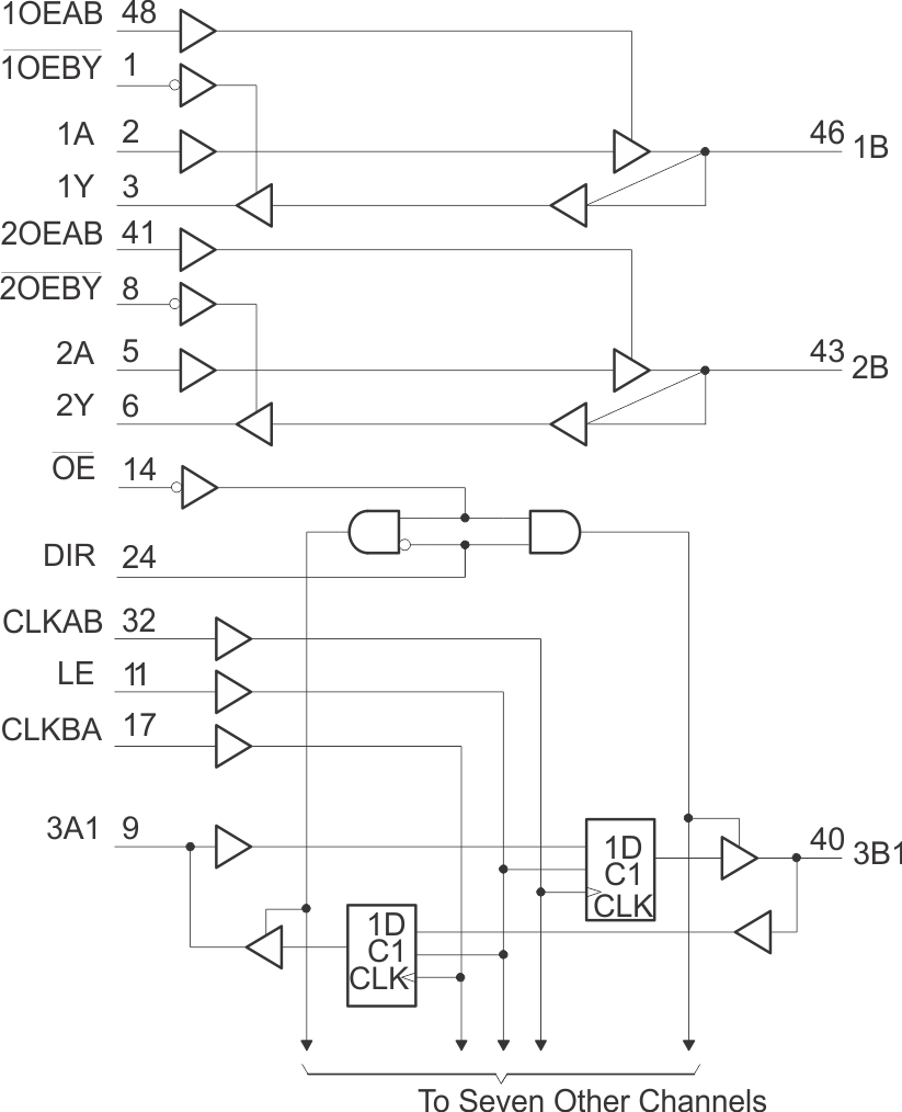
Logic Diagram (Positive Logic)

4 Revision History
Changes from * Revision (February 2005) to A Revision
- Added ESD Ratings table, Feature Description section, Device Functional Modes, Application and Implementation section, Power Supply Recommendations section, Layout section, Device and Documentation Support section, and Mechanical, Packaging, and Orderable Information section Go
- Removed Ordering Information table. Go
- Added junction temperature and removed package thermal impedance from Absolute Maximum Ratings Go
- Added different conditions and results for I and M versions to the Specifications Go
- Updated the VCC test condition for IOZ(PU/PD) Go
- Added Community Resources Go
5 Description (continued)
The SN74VMEH22501A-EP device is pin-for-pin compatible to the SN74VMEH22501 device (SCES357), but operates at a wider operating temperature range.
High-speed backplane operation is a direct result of the improved OEC circuitry and high drive that has been designed and tested into the VME64x backplane model. The B-port I/Os are optimized for driving large capacitive loads and include pseudo-ETL input thresholds (½ VCC ±50 mV) for increased noise immunity. These specifications support the 2eVME protocols in VME64x (ANSI/VITA 1.1) and 2eSST protocols in VITA 1.5.
With proper design of a 21-slot VME system, a designer can achieve 320-MB transfer rates on linear backplanes and, possibly, 1-GB transfer rates on the VME320 backplane.
All inputs and outputs are 5-V tolerant and are compatible with TTL and 5-V CMOS inputs.
Active bus-hold circuitry holds unused or undriven 3A-port inputs at a valid logic state. Bus-hold circuitry is not provided on 1A or 2A inputs, any B-port input, or any control input. Use of pullup or pulldown resistors with the bus-hold circuitry is not recommended.
This device is fully specified for live-insertion applications using Ioff, power-up 3-state, and BIAS VCC. The Ioff circuitry prevents damaging current to backflow through the device when it is powered off/on. The power-up 3-state circuitry places the outputs in the high-impedance state during power up and power down, which prevents driver conflict. The BIAS VCC circuitry precharges and preconditions the B-port input/output connections, preventing disturbance of active data on the backplane during card insertion or removal, and permits true live-insertion capability.
When VCC is between 0 and 1.5 V, the device is in the high-impedance state during power up or power down. However, to ensure the high-impedance state above 1.5 V, output-enable (OE and OEBY) inputs should be tied to VCC through a pullup resistor and output-enable (OEAB) inputs should be tied to GND through a pulldown resistor; the minimum value of the resistor is determined by the drive capability of the device connected to this input.
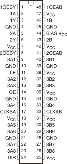
6 Pin Configuration and Functions

Pin Functions
| PIN | I/O | DESCRIPTION | |
|---|---|---|---|
| NAME | NO. | ||
| 1OEBY | 1 | I | Active low control output for 1Y bus |
| 1A | 2 | I | Data in to 1B |
| 1Y | 3 | O | Data out |
| GND | 4 | — | Ground |
| 2A | 5 | I | Data in to 2B |
| 2Y | 6 | O | Data out |
| VCC | 7 | I | Power supply input for internal circuits |
| 2OEBY | 8 | I | Active low control output for 2Y bus |
| 3A1 | 9 | I/O | Data in/out |
| GND | 10 | — | Ground |
| LE | 11 | I | Latch Enable pin for UBT |
| 3A2 | 12 | I/O | Data in/out |
| 3A3 | 13 | I/O | Data in/out |
| OE | 14 | I | Active low enable pin for UBT |
| GND | 15 | — | Ground |
| 3A4 | 16 | I/O | Data in/out |
| CLKBA | 17 | I | Clock for 3B data to 3A bus |
| VCC | 18 | I | Power supply input for internal circuits |
| 3A5 | 19 | I/O | Data in/out |
| 3A6 | 20 | I/O | Data in/out |
| GND | 21 | — | Ground |
| 3A6 | 22 | I/O | Data in/out |
| 3A8 | 23 | I/O | Data in/out |
| DIR | 24 | — | Direction control for UBT |
| VCC | 25 | I | Power supply input for internal circuits |
| 3B8 | 26 | I/O | Data in/out |
| 3B7 | 27 | I/O | Data in/out |
| GND | 28 | — | Ground |
| 3B6 | 29 | I/O | Data in/out |
| 3B5 | 30 | I/O | Data in/out |
| VCC | 31 | I | Power supply input for internal circuits |
| CLKAB | 32 | I | Clock for 3A data to 3B bus |
| 3B4 | 33 | I/O | Data in/out |
| GND | 34 | — | Ground |
| VCC | 35 | I | Power supply input for internal circuits |
| 3B3 | 36 | I/O | Data in/out |
| 3B2 | 37 | I/O | Data in/out |
| VCC | 38 | I | Power supply input for internal circuits |
| GND | 39 | — | Ground |
| 3B1 | 40 | I/O | Data in/out |
| 2OEAB | 41 | I | Active high control output for 2B bus |
| VCC | 42 | I | Power supply input for internal circuits |
| 2B | 43 | I/O | Data in/out |
| BIAS VCC | 44 | I | Power supply input for internal circuits |
| GND | 45 | — | Ground |
| 1B | 46 | I/O | Data in/out |
| VCC | 47 | I | Power supply input for internal circuits |
| 1OEAB | 48 | I | Active high control output for 1B bus |