-
SN75DP130 DisplayPort™ 1:1 Redriver With Link Training
- 1 Features
- 2 Applications
- 3 Description
- 4 Revision History
- 5 Description (continued)
- 6 Pin Configuration and Functions
- 7 Specifications
- 8 Parameter Measurement Information
- 9 Detailed Description
- 10Application and Implementation
- 11Power Supply Recommendations
- 12Layout
- 13Device and Documentation Support
- 14Mechanical, Packaging, and Orderable Information
- IMPORTANT NOTICE
Package Options
Mechanical Data (Package|Pins)
- RGZ|48
Thermal pad, mechanical data (Package|Pins)
- RGZ|48
Orderable Information
SN75DP130 DisplayPort™ 1:1 Redriver With Link Training
1 Features
- Supports DP v1.1a and DP v1.2 Signaling Including HBR2 Data Rates to 5.4 Gbps
- Supports HDMI 1.4b With TMDS Clock Frequencies up to 340 MHz
- Glueless Interface to AMD, Intel, and NVIDIA Graphics Processors
- Auto-Configuration Through Link Training
- Output Signal Conditioning With Tunable Voltage Swing and Pre-Emphasis Gain
- Highly Configurable Input Variable Equalizer
- Two Device Options Including a Dual Power Supply Configuration for Lowest Power
- 2-kV ESD HBM Protection
- Temperature Range: 0°C to 85°C
- 48-Pin 7-mm × 7-mm VQFN Package
2 Applications
- Notebook PCs
- Desktop PCs
- PC Docking Stations
- PC Standalone Video Cards
3 Description
The SN75DP130 device is a single channel DisplayPort™ (DP) re-driver that regenerates the DP high-speed digital link. The device complies with the VESA DisplayPort Standard Version 1.2, and supports a 4-lane Main Link interface signaling up to HBR2 rates at 5.4 Gbps per lane. This device also supports DP++ Dual-Mode, offering TMDS signaling for DVI and full HDMI Version 1.4a support.
The device compensates for PCB-related frequency loss and switching-related loss to provide the optimum DP electrical performance from source to sink. The Main Link signal inputs feature configurable equalizers with selectable boost settings. At the Main Link output, four primary levels of differential output voltage swing (VOD) and four primary levels of pre-emphasis are available. A secondary level of boost adjustment, programmed through I2C, for fine-tuning the Main Link output. The device can monitor the AUX channel and automatically adjust the output signaling levels and input equalizers in response to Link Training commands. Additionally, the SN75DP130 output signal conditioning and EQ parameters are fully programmable through the I2C interface.
Device Information(1)
| PART NUMBER | PACKAGE | BODY SIZE (NOM) |
|---|---|---|
| SN75DP130 | VQFN (48) | 7.00 mm × 7.00 mm |
- For all available packages, see the orderable addendum at the end of the data sheet.
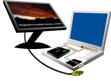
Simple Application

4 Revision History
Changes from D Revision (July 2013) to E Revision
- Added Pin Configuration and Functions section, ESD Ratings table, Feature Description section, Device Functional Modes, Application and Implementation section, Power Supply Recommendations section, Layout section, Device and Documentation Support section, and Mechanical, Packaging, and Orderable Information section Go
Changes from C Revision (January 2013) to D Revision
- Power-Down Sequence deleted: 1. De-assert EN to the deviceGo
- Power-Up Sequence deleted: 1. Assert RSTN and de-assert EN to the device.Go
- Power-Up Sequence deleted: 5. Assert EN a minimum of 10 µs after RSTN has been de-asserted. Go
- Deleted the EN time line from Figure 34Go
Changes from B Revision (October 2011) to C Revision
- Added text to RSTN description in PIN FUNCTIONSGo
- Added RSTN pin row to VIH in RECOMMENDED OPERATING CONDITIONSGo
- Added RSTN pin row to VIL in RECOMMENDED OPERATING CONDITIONSGo
- Added rows to Device power under normal operation in POWER DISSIPATION tableGo
- Changed in Table 1 13.9 to 113.9Go
- Deleted unnecessary tie dot in Block DiagramGo
- Changed Table 3Go
- Changed Figure 17Go
- Changed Figure 18Go
- Changed SN75DP130 Local I2C Control and Status RegistersGo
- Added DP130 POWER SEQUENCING sectionGo
Changes from A Revision (September 2011) to B Revision
- Deleted pins 37 an 43 from GND in the PIN FUNCTIONS tableGo
Changes from * Revision (April 2011) to A Revision
- Changed pin numbers in PIN FUNCTIONS table, VDDD_DREG and NCGo
5 Description (continued)
The SN75DP130 is optimized for mobile applications, and contains activity detection circuitry on the Main Link input that transitions to a low-power Output Disable mode in the absence of a valid input signal. Other low-power modes are supported, including a standby mode with typical dissipation of approximately 2 mW when no video sink (for example, monitor) is connected.
The device is characterized for an extended operational temperature range from 0°C to 85°C.
The SN75DP130 offers separate AUX and DDC source interfaces that connect to one AUX sink channel. This minimizes component count when implemented with a graphics processor (GPU) comprising separate DDC and AUX interfaces. For GPUs with combined DDC/AUX, the device can operate as a FET switch to short-circuit the AUX channel AC coupling caps while connected to a TMDS sink device. Other sideband circuits such as Hot Plug Detect (HPD) are optimized to reduce external components, providing a seamless connection to Intel, AMD, and NVIDIA graphics processors.
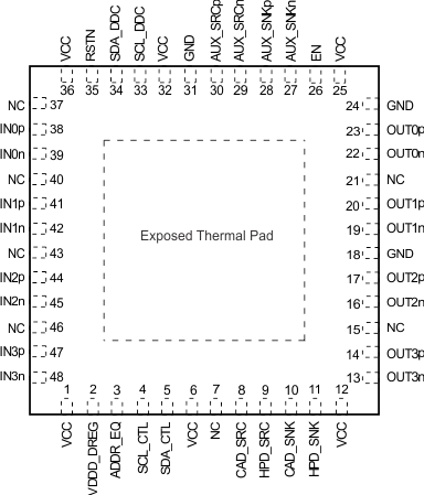
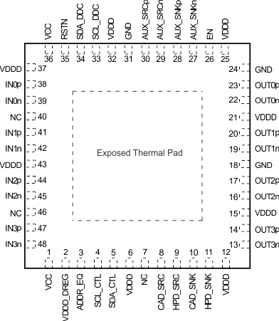
6 Pin Configuration and Functions


Pin Functions
| PIN | I/O | DESCRIPTION | |
|---|---|---|---|
| NAME | NO. | ||
| MAIN LINK TERMINALS | |||
| IN0n | 39 | Input (100-Ω diff) |
DisplayPort Main Link Lane 0 Differential Input |
| IN0p | 38 | ||
| IN1n | 42 | DisplayPort Main Link Lane 1 Differential Input | |
| IN1p | 41 | ||
| IN2n | 45 | DisplayPort Main Link Lane 2 Differential Input | |
| IN2p | 44 | ||
| IN3n | 48 | DisplayPort Main Link Lane 3 Differential Input | |
| IN3p | 47 | ||
| OUT0n | 22 | Output (100-Ω diff) |
DisplayPort Main Link Lane 0 Differential Output |
| OUT0p | 23 | ||
| OUT1n | 19 | DisplayPort Main Link Lane 1 Differential Output | |
| OUT1p | 20 | ||
| OUT2n | 16 | DisplayPort Main Link Lane 2 Differential Output | |
| OUT2p | 17 | ||
| OUT3n | 13 | DisplayPort Main Link Lane 3 Differential Output | |
| OUT3p | 14 | ||
| AUX CHANNEL AND DDC DATA TERMINALS | |||
| AUX_SRCn | 29 | I/O (100-Ω diff) |
Source Side Bidirectional DisplayPort Auxiliary Data Channel. If the AUX_SNK channel is used for monitoring only, these signals are not used and may be left open. |
| AUX_SRCp | 30 | ||
| AUX_SNKn | 27 | I/O (100-Ω diff) |
Sink Side Bidirectional DisplayPort Auxiliary Data Channel. |
| AUX_SNKp | 28 | ||
| SDA_DDC | 34 | I/O | Bidirectional I2C Display Data Channel (DDC) for TMDS mode. These signals may be used together with AUX_SNK to form a FET switch to short-circuit the AC coupling capacitors during TMDS operation in a DP++ Dual-Mode configuration. These terminals include integrated 60-kΩ pullup resistors |
| SCL_DDC | 33 | ||
| HPD, CAD, AND CONTROL TERMINALS | |||
| HPD_SRC | 9 | O | Hot Plug Detect Output to the DisplayPort Source. |
| HPD_SNK | 11 | I | DisplayPort Hot Plug Detect Input from Sink. This device input is 5-V tolerant. |
| Note: Pull this input high during compliance testing or use I2C control interface to go into compliance test mode and control HPD_SNK and HPD_SRC by software. | |||
| CAD_SRC | 8 | O | DP Cable Adapter Detect Output. This output typically drives the GPU CAD input. |
| CAD_SNK | 10 | I | DisplayPort Cable Adapter Detect Input. This input tolerates a 5-V supply with a supply impedance higher than 90kΩ. A device internal zener diode limits the input voltage to 3.3 V. An external 1MΩ resistor to GND is recommended. This terminal is used to select DP mode or TMDS mode in a DP++ Dual-Mode application. |
| SCL_CTL | 4 | I/O | Bidirectional I2C interface to configure the SN75DP130. This interface is active independent of the EN input but inactive when RSTN is low. |
| SDA_CTL | 5 | ||
| RSTN | 35 | I | Active Low Device Reset. This input includes a 150-kΩ resistor to the VDDD core supply. An external capacitor to GND is recommended on the RSTN input to provide a power-up delay (see the VIL and VIH specifications in Recommended Operating Conditions). |
| This signal is used to place the SN75DP130 into Shutdown mode for the lowest power consumption. When the RSTN input is asserted, all outputs (excluding HPD_SRC and CAD_SRC) are high-impedance, and inputs (excluding HPD_SNK and CAD_SNK) are ignored; all I2C and DPCD registers are reset to their default values. | |||
| At power up, the RSTN input must not be de-asserted until the VCC and VDDD supplies have reached at least the minimum recommended supply voltage level (see Figure 34 for timing requirements). | |||
| EN | 26 | I | Device Enable. This input incorporates an internal pullup of 200 kΩ. |
| ADDR_EQ | 3 | 3-level Input | I2C Target Address Select and EQ Configuration Input. If the I2C bus is used, this input setting selects the I2C target address, as described in Figure 19. This input also configures the input EQ to the device, as described in Table 3. |
| SUPPLY AND GROUND TERMINALS | |||
| VDDD | SN75DP130DS
6, 12, 15, 21, 25, 32, 37, 43 |
Digital low voltage core and Main Link supply for SN75DP130DS device option. Nominally 1.1 V. |
|
| VCC | SN75DP130SS
1, 6, 12, 25, 32, 36 |
3.3-V Supply | |
| SN75DP130DS
1, 36 |
|||
| VDDD_DREG | 2 | SN75DP130SS: Digital voltage regulator decoupling; install 1 µF to GND. SN75DP130DS: Treat same as VDDD; this pin will be most noisy of all VDDD terminals and needs a decoupling capacitor nearby. |
|
| GND | 18, 24, 31, and Exposed Thermal Pad |
Ground. Reference GND connections include the device package exposed thermal pad. | |
| NC | SN75DP130SS
7, 15, 21, 37, 40, 43, 46 |
No Connect. These terminals may be left unconnected, or connect to GND. | |
| SN75DP130DS
7, 40, 46 |
|||