-
TLIN2022A-Q1 Dual Local Interconnect Network (LIN) Transceiver with Dominant State Timeout
- 1 Features
- 2 Applications
- 3 Description
- 4 Description (Continued)
- 5 Revision History
- 6 Pin Configuration and Functions
- 7 Specifications
- 8 Parameter Measurement Information
-
9 Detailed Description
- 9.1 Overview
- 9.2 Functional Block Diagram
- 9.3
Feature Description
- 9.3.1 LIN (Local Interconnect Network) Bus
- 9.3.2 TXD
- 9.3.3 RXD (Receive Output)
- 9.3.4 VSUP (Supply Voltage)
- 9.3.5 GND (Ground)
- 9.3.6 EN (Enable Input)
- 9.3.7 Protection Features
- 9.3.8 TXD Dominant Time Out (DTO)
- 9.3.9 Bus Stuck Dominant System Fault: False Wake-Up Lockout
- 9.3.10 Thermal Shutdown
- 9.3.11 Undervoltage on VSUP
- 9.3.12 Unpowered Device and LIN Bus
- 9.4 Device Functional Modes
- 10Application Information Disclaimer
- 11Layout
- 12Device and Documentation Support
- 13Mechanical, Packaging, and Orderable Information
- IMPORTANT NOTICE
Package Options
Mechanical Data (Package|Pins)
Thermal pad, mechanical data (Package|Pins)
- DMT|14
Orderable Information
TLIN2022A-Q1 Dual Local Interconnect Network (LIN) Transceiver with Dominant State Timeout
1 Features
- AEC-Q100 (grade 1) qualified for automotive applications
- Compliant to LIN 2.0, LIN 2.1, LIN 2.2, LIN 2.2 A and ISO/DIS 17987–4 electrical physical layer (EPL) specification
- Conforms to SAE J2602-1 LIN network for vehicle applications
- Functional Safety-Capable
- Supports 12-V and 24-V battery applications
- LIN transmit data rate up to 20 kbps
- LIN receive data rate up to 100 kbps
- Wide operational supply voltage range from 4 V to 48 V
- Sleep mode: ultra-low current consumption allows
wake-up event from:
- LIN bus
- Local wake up through EN
- Power up and power down glitch-free operation on LIN bus and RXD output
- Protection
features:
- ±60 V LIN bus fault tolerant
- Undervoltage protection on VSUP
- TXD Dominant time out protection (DTO)
- Thermal shutdown protection
- Unpowered node or ground disconnection failsafe at system level.
- Available in SOIC (14) package and leadless VSON (14) Package with wettable flanks
3 Description
The TLIN2022A-Q1 is a Dual Local Interconnect Network (LIN) physical layer transceiver with integrated wake-up and protection features, compliant with LIN 2.0, LIN 2.1, LIN 2.2, LIN 2.2A and ISO/DIS 17987–4 standards. LIN is a single wire bidirectional bus typically used for low speed in-vehicle networks using data rates up to 20 kbps. The TLIN2022A-Q1 is designed to support 12-V and 24-V applications with wider operating voltage and additional bus-fault protection.
The LIN receiver supports data rates up to 100 kbps for faster in-line programming. The TLIN2022A-Q1 converts the LIN protocol data stream on the TXD input into a LIN bus signal using a current-limited wave-shaping driver which reduces electromagnetic emissions (EME). The receiver converts the data stream to logic-level signals that are sent to the microprocessor through the open-drain RXD pin. Ultra-low current consumption is possible using the sleep mode which allows wake-up via LIN bus or EN pin.
| PART NUMBER | PACKAGE(1) | BODY SIZE (NOM) |
|---|---|---|
| TLIN2022A-Q1 | SOIC (14) (D) | 5.00 mm x 8.65 mm |
| VSON (14) (DMT) | 3.00 mm x 4.50 mm |
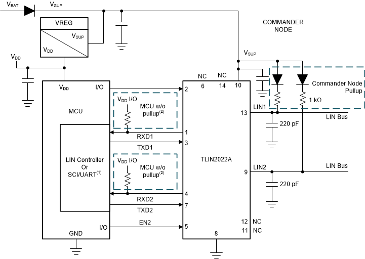
 Simplified Schematics, Commander Mode
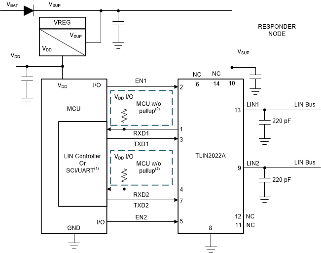
 Simplified Schematics, Responder Mode
4 Description (Continued)
5 Revision History
| DATE | REVISION | NOTES |
|---|---|---|
| June 2021 | * | Initial release |
6 Pin Configuration and Functions
| PIN | Type | DESCRIPTION | |
|---|---|---|---|
| NO. | NAME | ||
| 1 | RXD1 | O | Channel 1 RXD Output (open-drain) interface reporting state of LIN bus voltage |
| 2 | EN1 | I | Channel 1 Enable Input- High puts the channel 1 in normal operation mode and low puts it in sleep mode |
| 3 | TXD1 | I | Channel 1 TXD input interface to control state of LIN output |
| 4 | RXD2 | O | Channel 2 RXD Output (open-drain) interface reporting state of LIN bus voltage |
| 5 | EN2 | I | Channel 2 Enable Input- High puts the channel 2 in normal operation mode and low puts it in sleep mode |
| 7 | TXD2 | I | Channel 2 TXD input interface to control state of LIN output |
| 8 | GND | GND | Ground |
| 9 | LIN2 | HV I/O | Channel 2 High voltage LIN bus single-wire transmitter and receiver |
| 10 | VSUP | Supply | Device Supply Voltage (connected to battery in series with external reverse blocking diode) |
| 13 | LIN1 | HV I/O | Channel 1 High voltage LIN bus single-wire transmitter and receiver |
| 6, 11, 12, 14 |
NC | – | Not Connected |
| Thermal Pad | – | Can be connected to the PCB ground plane to improve thermal coupling (DMT package only) | |
7 Specifications
7.1 Absolute Maximum Ratings
| Symbol | Parameter | MIN | MAX | UNIT |
|---|---|---|---|---|
| VSUP | Supply voltage range (ISO/DIS 17987 Param 10) | –0.3 | 60 | V |
| VLIN | LIN bus input voltage (ISO/DIS 17987 Param 82) | –60 | 60 | V |
| VLOGIC | Logic pin voltage (RXD, TXD, EN) | –0.3 | 6 | V |
| IO | Logic pin output current | 8 | mA | |
| TJ | Junction temperature range | –55 | 150 | °C |