-
TLVx171 36-V, Single-Supply, Low-Power Operational Amplifiers for Cost-Sensitive Systems
- 1 Features
- 2 Applications
- 3 Description
- 4 Revision History
- 5 Pin Configuration and Functions
- 6 Specifications
- 7 Detailed Description
- 8 Application and Implementation
- 9 Power Supply Recommendations
- 10Layout
- 11Device and Documentation Support
- 12Mechanical, Packaging, and Orderable Information
- IMPORTANT NOTICE
Package Options
Mechanical Data (Package|Pins)
Thermal pad, mechanical data (Package|Pins)
Orderable Information
TLVx171 36-V, Single-Supply, Low-Power Operational Amplifiers for Cost-Sensitive Systems
1 Features
- Supply Range: 2.7 V to 36 V, ±1.35 V to ±18 V
- Low Noise: 16 nV/√Hz
- Low Offset Drift: ±1 μV/°C (typical)
- EMI-Hardened with RFI-Filtered Inputs
- Input Range Includes the Negative Supply
- Unity-Gain Stable: 200-pF Capacitive Load
- Rail-to-Rail Output
- Gain Bandwidth: 3 MHz
- Low Quiescent Current: 525 µA per Amplifier
- High Common-Mode Rejection: 105 dB (typical)
- Low Bias Current: 10 pA
2 Applications
- Transducers
- Currency Counters
- AC-DC Converters
- Power Modules
- Inverters
- Test Equipment
- Battery-Powered Instruments
- TFT-LCD Drive Circuits
- Active Filters
3 Description
The 36-V TLVx171 family provides a low-power option for cost-conscious industrial and personal electronics systems requiring an electromagnetic interference (EMI)-hardened, low-noise, single-supply operational amplifier (op amp) that operates on supplies ranging from 2.7 V (±1.35 V) to 36 V (±18 V). The single-channel TLV171, dual-channel TLV2171, and quad-channel TLV4171 provide low offset, drift, quiescent current balanced with high bandwidth for the power. The devices are available in micropackages for space-constrained systems and feature identical specifications for maximum design flexibility.
Unlike most op amp, which are specified at only one supply voltage, the TLVx171 family is specified from 2.7 V to 36 V. Input signals beyond the supply rails do not cause phase reversal. The TLVx171 family is stable with capacitive loads up to 200 pF. The input can operate 100 mV below the negative rail and within 2 V of the top rail during normal operation. These devices can operate with a full rail-to-rail input 100 mV beyond the top rail, but with reduced performance within 2 V of the top rail.
The TLVx171 op amp family is specified from –40°C to +125°C.
Device Information(1)
| PART NUMBER | PACKAGE | BODY SIZE (NOM) |
|---|---|---|
| TLV171 | SOIC (8) | 4.90 mm × 3.91 mm |
| SOT-23 (5) | 2.90 mm × 1.60 mm | |
| TLV2171 | SOIC (8) | 4.90 mm × 3.91 mm |
| VSSOP (8) | 3.00 mm × 3.00 mm | |
| TLV4171 | SOIC (14) | 8.65 mm × 3.91 mm |
| TSSOP (14) | 5.00 mm × 4.40 mm |
- For all available packages, see the orderable addendum at the end of the data sheet.
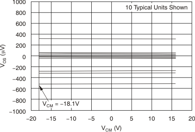
Offset Voltage vs Common-Mode Voltage
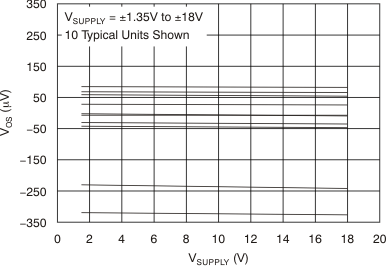
Offset Voltage vs Power Supply
4 Revision History
| DATE | REVISION | NOTES |
|---|---|---|
| September 2016 | * | Initial release. |
5 Pin Configuration and Functions
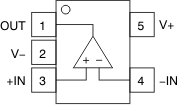
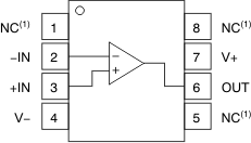
Pin Functions: TLV171
| PIN | I/O | DESCRIPTION | ||
|---|---|---|---|---|
| NAME | TLV171 | |||
| DBV | D | |||
| IN– | 4 | 2 | I | Negative (inverting) input |
| IN+ | 3 | 3 | I | Positive (noninverting) input |
| NC(1) | — | 1, 5, 8 | — | No internal connection (can be left floating) |
| OUT | 1 | 6 | O | Output |
| V+ | 5 | 7 | — | Positive (highest) power supply |
| V– | 2 | 4 | — | Negative (lowest) power supply |
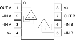
Pin Functions: TLV2171
| PIN | I/O | DESCRIPTION | ||
|---|---|---|---|---|
| NAME | TLV2171 | |||
| D | DGK | |||
| –IN A | 2 | 2 | I | Inverting input, channel A |
| –IN B | 6 | 6 | I | Inverting input, channel B |
| +IN A | 3 | 3 | I | Noninverting input, channel A |
| +IN B | 5 | 5 | I | Noninverting input, channel B |
| OUT A | 1 | 1 | O | Output, channel A |
| OUT B | 7 | 7 | O | Output, channel B |
| V– | 4 | 4 | — | Negative (lowest) power supply |
| V+ | 8 | 8 | — | Positive (highest) power supply |
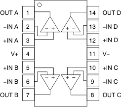
Pin Functions: TLV4171
| PIN | I/O | DESCRIPTION | ||
|---|---|---|---|---|
| NAME | D | PW | ||
| –IN A | 2 | 2 | I | Inverting input, channel A |
| +IN A | 3 | 3 | I | Noninverting input, channel A |
| –IN B | 6 | 6 | I | Inverting input, channel B |
| +IN B | 5 | 5 | I | Noninverting input, channel B |
| –IN C | 9 | 9 | I | Inverting input, channel C |
| +IN C | 10 | 10 | I | Noninverting input, channel C |
| –IN D | 13 | 13 | I | Inverting input, channel D |
| +IN D | 12 | 12 | I | Noninverting input, channel D |
| OUT A | 1 | 1 | O | Output, channel A |
| OUT B | 7 | 7 | O | Output, channel B |
| OUT C | 8 | 8 | O | Output, channel C |
| OUT D | 14 | 14 | O | Output, channel D |
| V– | 11 | 11 | — | Negative (lowest) power supply |
| V+ | 4 | 4 | — | Positive (highest) power supply |
6 Specifications
6.1 Absolute Maximum Ratings
Over operating free-air temperature range, unless otherwise noted.(1)| MIN | MAX | UNIT | ||
|---|---|---|---|---|
| Voltage | Supply voltage, V+ to V− | –20 | 20 | V |
| Signal input pin | (V−) − 0.5 | (V+) + 0.5 | ||
| Current | Signal input pin | –10 | 10 | mA |
| Output short-circuit(2) | Continuous | |||
| Temperature | Operating, TA | –55 | 150 | °C |
| Junction, TJ | 150 | |||
| Storage, Tstg | –65 | 150 | ||
6.2 ESD Ratings
| VALUE | UNIT | |||
|---|---|---|---|---|
| V(ESD) | Electrostatic discharge | Human-body model (HBM), per ANSI/ESDA/JEDEC JS-001(1) | ±4000 | V |
| Charged-device model (CDM), per JEDEC specification JESD22-C101(2) | ±750 | |||
6.3 Recommended Operating Conditions
over operating free-air temperature range (unless otherwise noted)| MIN | NOM | MAX | UNIT | ||
|---|---|---|---|---|---|
| Supply voltage (V+ – V–) | Single supply | 2.7 | 36 | V | |
| Dual supply | ±1.35 | ±18 | |||
| Specified temperature | –40 | +125 | °C | ||
6.4 Thermal Information: TLV171
| THERMAL METRIC(1) | TLV171 | UNIT | ||
|---|---|---|---|---|
| D (SOIC) | DBV (SOT-23) | |||
| 8 PINS | 5 PINS | |||
| RθJA | Junction-to-ambient thermal resistance | 149.5 | 245.8 | °C/W |
| RθJC(top) | Junction-to-case (top) thermal resistance | 97.9 | 133.9 | °C/W |
| RθJB | Junction-to-board thermal resistance | 87.7 | 83.6 | °C/W |
| ψJT | Junction-to-top characterization parameter | 35.5 | 18.2 | °C/W |
| ψJB | Junction-to-board characterization parameter | 89.5 | 83.1 | °C/W |
| RθJC(bot) | Junction-to-case (bottom) thermal resistance | — | — | °C/W |
6.5 Thermal Information: TLV2171
| THERMAL METRIC(1) | TLV2171 | UNIT | ||
|---|---|---|---|---|
| D (SOIC) | DGK (VSSOP) | |||
| 8 PINS | 8 PINS | |||
| RθJA | Junction-to-ambient thermal resistance | 134.3 | 175.2 | °C/W |
| RθJC(top) | Junction-to-case (top) thermal resistance | 72.1 | 74.9 | °C/W |
| RθJB | Junction-to-board thermal resistance | 60.6 | 22.2 | °C/W |
| ψJT | Junction-to-top characterization parameter | 18.2 | 1.6 | °C/W |
| ψJB | Junction-to-board characterization parameter | 53.8 | 22.8 | °C/W |
| RθJC(bot) | Junction-to-case (bottom) thermal resistance | — | — | °C/W |
6.6 Thermal Information: TLV4171
| THERMAL METRIC(1) | TLV4171 | UNIT | ||
|---|---|---|---|---|
| D (SOIC) | PW (TSSOP) | |||
| 14 PINS | 14 PINS | |||
| RθJA | Junction-to-ambient thermal resistance | 93.2 | 106.9 | °C/W |
| RθJC(top) | Junction-to-case (top) thermal resistance | 51.8 | 24.4 | °C/W |
| RθJB | Junction-to-board thermal resistance | 49.4 | 59.3 | °C/W |
| ψJT | Junction-to-top characterization parameter | 13.5 | 0.6 | °C/W |
| ψJB | Junction-to-board characterization parameter | 42.2 | 54.3 | °C/W |
| RθJC(bot) | Junction-to-case (bottom) thermal resistance | — | — | °C/W |
6.7 Electrical Characteristics
at TA = 25°C, VCM = VOUT = VS / 2, and RL = 10 kΩ connected to VS / 2 (unless otherwise noted)| PARAMETER | TEST CONDITIONS | MIN | TYP | MAX | UNIT | |
|---|---|---|---|---|---|---|
| OFFSET VOLTAGE | ||||||
| VOS | Input offset voltage | TA = 25°C | 0.75 | ±2.7 | mV | |
| TA = –40°C to +125°C | ±3.0 | |||||
| dVOS/dT | Input offset voltage drift | TA = –40°C to +125°C | 1 | µV/°C | ||
| PSRR | Input offset voltage vs power supply | VS = 4 V to 36 V, TA = –40°C to +125°C | 90 | 105 | dB | |
| INPUT BIAS CURRENT | ||||||
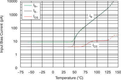
| IB | Input bias current | ±10 | pA | |||
| IOS | Input offset current | ±4 | pA | |||
| NOISE | ||||||
| Input voltage noise | f = 0.1 Hz to 10 Hz | 3 | µVPP | |||
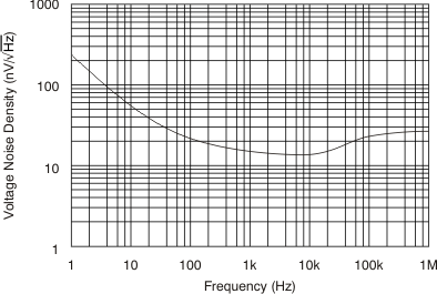
| en | Input voltage noise density | f = 100 Hz | 27 | nV/√Hz | ||
| f = 1 kHz | 16 | |||||
| INPUT VOLTAGE | ||||||
| VCM | Common-mode voltage range(1) | (V–) – 0.1 | (V+) – 2 | V | ||
| CMRR | Common-mode rejection ratio | VS = ±18 V, (V–) – 0.1 V < VCM < (V+) – 2 V, TA = –40°C to +125°C |
94 | 105 | dB | |
| INPUT IMPEDANCE | ||||||
| Differential | 100 || 3 | MΩ || pF | ||||
| Common-mode | 6 || 3 | 1012 Ω || pF | ||||
| OPEN-LOOP GAIN | ||||||
| AOL | Open-loop voltage gain | VS = 36 V, (V–) + 0.35 V < VO < (V+) – 0.35 V, TA = –40°C to +125°C |
94 | 130 | dB | |
| FREQUENCY RESPONSE | ||||||
| GBP | Gain bandwidth product | 3.0 | MHz | |||
| SR | Slew rate | G = +1 | 1.5 | V/µs | ||
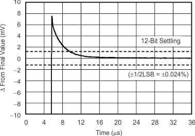
| tS | Settling time | To 0.1%, VS = ±18 V, G = +1, 10-V step | 6 | µs | ||
| To 0.01% (12 bits), VS = ±18 V, G = +1, 10-V step |
10 | |||||
| Overload recovery time | VIN × gain > VS | 2 | µs | |||
| THD+N | Total harmonic distortion + noise | G = +1, f = 1 kHz, VO = 3 VRMS | 0.0002% | |||
| OUTPUT | ||||||
| VO | Voltage output swing | Positive rail, VS = ±18 V, RL = 10 kΩ, TA = 25°C |
160 | mV | ||
| Negative rail, VS = ±18 V, RL = 10 kΩ, TA = 25°C |
90 | mV | ||||
| RL = 10 kΩ, AOL ≥ 94 dB, TA = –40°C to +125°C |
(V–) + 0.35 | (V+) – 0.35 | V | |||
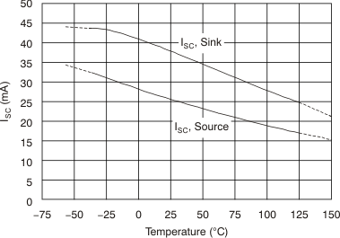
| ISC | Short-circuit current | 25 | mA | |||
| –35 | ||||||
| CLOAD | Capacitive load drive | See Typical Characteristics | pF | |||
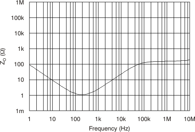
| RO | Open-loop output resistance | f = 1 MHz, IO = 0 A | 150 | Ω | ||
| POWER SUPPLY | ||||||
| VS | Specified voltage range | 2.7 | 36 | V | ||
| IQ | Quiescent current per amplifier | IO = 0 A, TA = –40°C to +125°C | 525 | 695 | µA | |
| TEMPERATURE | ||||||
| Specified range | –40 | 125 | °C | |||
| Operating range | –55 | 150 | °C | |||
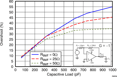
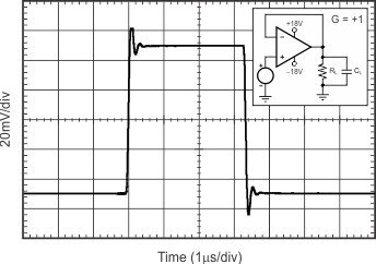
6.8 Typical Characteristics
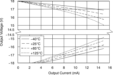
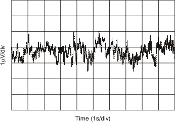
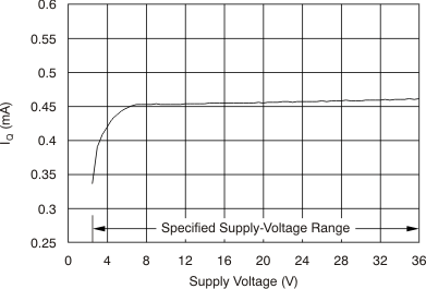
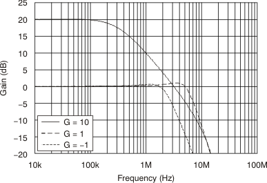
at VS = ±18 V, VCM = VS / 2, RLOAD = 10 kΩ connected to VS / 2, and CL = 100 pF (unless otherwise noted)Table 1. Characteristic Performance Measurements
| DESCRIPTION | FIGURE |
|---|---|
| Offset Voltage Production Distribution | Figure 1 |
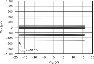
| Offset Voltage vs Common-Mode Voltage | Figure 2 |
| Offset Voltage vs Common-Mode Voltage (Upper Stage) | Figure 3 |
| Input Bias Current and Input Offset Current vs Temperature | Figure 4 |
| Output Voltage Swing vs Output Current (Maximum Supply) | Figure 5 |
| CMRR and PSRR vs Frequency (Referred-to-Input) | Figure 6 |
| 0.1-Hz to 10-Hz Noise | Figure 7 |
| Input Voltage Noise Spectral Density vs Frequency | Figure 8 |
| Quiescent Current vs Supply Voltage | Figure 9 |
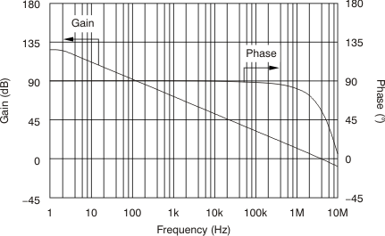
| Open-Loop Gain and Phase vs Frequency | Figure 10 |
| Closed-Loop Gain vs Frequency | Figure 11 |
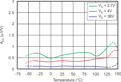
| Open-Loop Gain vs Temperature | Figure 12 |
| Open-Loop Output Impedance vs Frequency | Figure 13 |
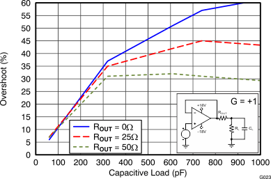
| Small-Signal Overshoot vs Capacitive Load | Figure 14, Figure 15 |
| No Phase Reversal | Figure 16 |
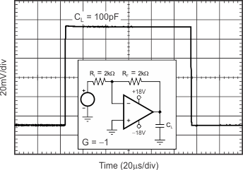
| Small-Signal Step Response (100 mV) | Figure 17, Figure 18 |
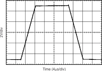
| Large-Signal Step Response | Figure 19, Figure 20 |
| Large-Signal Settling Time (10-V Positive Step) | Figure 21 |
| Large-Signal Settling Time (10-V Negative Step) | Figure 22 |
| Short-Circuit Current vs Temperature | Figure 23 |
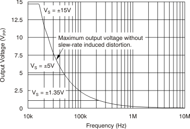
| Maximum Output Voltage vs Frequency | Figure 24 |
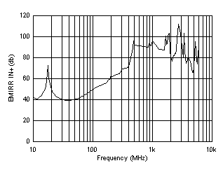
| EMIRR IN+ vs Frequency | Figure 25 |
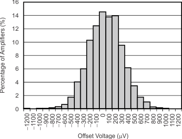
| Distribution taken from 3500 amplifiers |
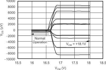
| 10 typical units shown |
(Upper Stage)
| 100-mV output step, RL = 10 kΩ |
| RL = 10 kΩ, CL = 100 pF |

| G = +1, RL = 10 kΩ, CL = 100 pF |
| 10-V positive step, G = –1 |
| 10 typical units shown |
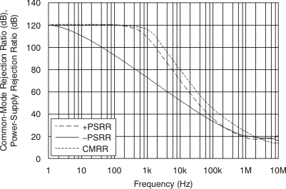
(Referred-to Input)
| 5 typical units shown |
| 100-mV output step, RL = 10 kΩ |
| G = –1, RL = 10 kΩ, CL = 100 pF |
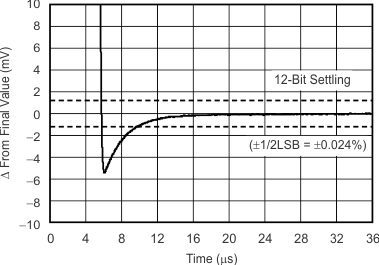
| 10-V negative step, G = –1 |
7 Detailed Description
7.1 Overview
The TLVx171 family of operational amplifiers provides high overall performance, making these devices ideal for many general-purpose applications. The excellent offset drift of only 2 μV/°C provides excellent stability over the entire temperature range. In addition, the device family offers very good overall performance with high common-mode rejection ratio (CMRR), power-supply rejection ratio (PSRR), and open-loop voltage gain (AOL).
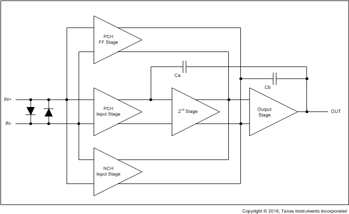
7.2 Functional Block Diagram
7.3 Feature Description
7.3.1 Operating Characteristics
The TLVx171 family of amplifiers is specified for operation from 2.7 V to 36 V, single supply (±1.35 V to ±18 V, dual supply). Many of the specifications apply from –40°C to +125°C. Parameters that can exhibit significant variance with regard to operating voltage or temperature are presented in the Typical Characteristics section.
7.3.2 Phase-Reversal Protection
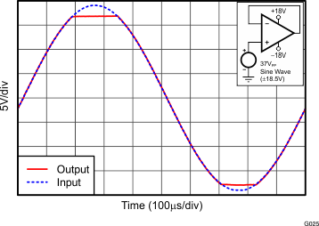
The TLVx171 family has an internal phase-reversal protection. Many operational amplifiers exhibit a phase reversal when the input is driven beyond the linear common-mode range. This condition is most often encountered in noninverting circuits when the input is driven beyond the specified common-mode voltage range, causing the output to reverse into the opposite rail. The input of the TLVx171 prevents phase reversal with excessive common-mode voltage. Instead, the output limits into the appropriate rail. This performance is shown in Figure 26.
 Figure 26. No Phase Reversal
7.3.3 Electrical Overstress
Designers often ask questions about the capability of an operational amplifier to withstand electrical overstress. These questions tend to focus on the device inputs, but can involve the supply voltage pins or even the output pin. Each of these different pin functions have electrical stress limits determined by the voltage breakdown characteristics of the particular semiconductor fabrication process and specific circuits connected to the pin. Additionally, internal electrostatic discharge (ESD) protection is built into these circuits for protection from accidental ESD events both before and during product assembly.
A good understanding of this basic ESD circuitry and the relevance to an electrical overstress event is helpful. Figure 27 illustrates the ESD circuits contained in the TLVx171 (indicated by the dashed line area). The ESD protection circuitry involves several current-steering diodes connected from the input and output pins and routed back to the internal power-supply lines, where the diodes meet at an absorption device internal to the operational amplifier. This protection circuitry is intended to remain inactive during normal circuit operation.
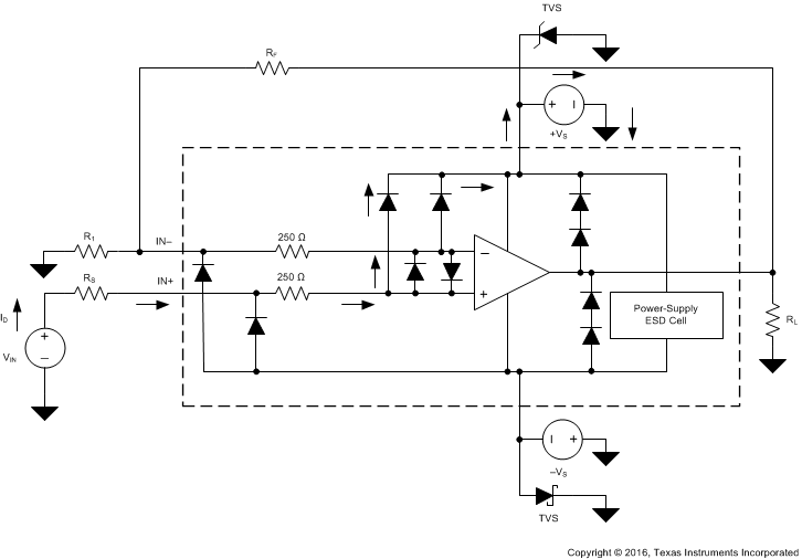 Figure 27. Equivalent Internal ESD Circuitry Relative to a Typical Circuit Application
An ESD event produces a short-duration, high-voltage pulse that is transformed into a short-duration, high-current pulse when discharging through a semiconductor device. The ESD protection circuits are designed to provide a current path around the operational amplifier core to prevent damage. The energy absorbed by the protection circuitry is then dissipated as heat.
When an ESD voltage develops across two or more amplifier device pins, current flows through one or more steering diodes. Depending on the path that the current takes, the absorption device can activate. The absorption device has a trigger, or threshold voltage, that is above the normal operating voltage of the TLVx171 but below the device breakdown voltage level. When this threshold is exceeded, the absorption device quickly activates and clamps the voltage across the supply rails to a safe level.
When the operational amplifier connects into a circuit (as shown in Figure 27), the ESD protection components are intended to remain inactive and do not become involved in the application circuit operation. However, circumstances may arise where an applied voltage exceeds the operating voltage range of a given pin. If this condition occurs, there is a risk that some internal ESD protection circuits can turn on and conduct current. Any such current flow occurs through steering-diode paths and rarely involves the absorption device.
Figure 27 shows a specific example where the input voltage (VIN) exceeds the positive supply voltage (V+) by 500 mV or more. Much of what happens in the circuit depends on the supply characteristics. If V+ can sink the current, one of the upper input steering diodes conducts and directs current to V+. Excessively high current levels can flow with increasingly higher VIN. As a result, the data sheet specifications recommend that applications limit the input current to 10 mA.
If the supply is not capable of sinking the current, VIN can begin sourcing current to the operational amplifier and then take over as the source of positive supply voltage. The danger in this case is that the voltage can rise to levels that exceed the operational amplifier absolute maximum ratings.
Another common question involves what happens to the amplifier if an input signal is applied to the input when the power supplies (V+ or V–) are at 0 V. Again, this question depends on the supply characteristic when at 0 V, or at a level below the input signal amplitude. If the supplies appear as high impedance, then the input source supplies the operational amplifier current through the current-steering diodes. This state is not a normal bias condition; most likely, the amplifier does not operate normally. If the supplies are low impedance, then the current through the steering diodes can become quite high. The current level depends on the ability of the input source to deliver current, and any resistance in the input path.
If there is any uncertainty about the ability of the supply to absorb this current, add external Zener diodes to the supply pins; see Figure 27. Select the Zener voltage so that the diode does not turn on during normal operation. However, the Zener voltage must be low enough so that the Zener diode conducts if the supply pin begins to rise above the safe-operating, supply-voltage level.
The TLVx171 input pins are protected from excessive differential voltage with back-to-back diodes; see Figure 27. In most circuit applications, the input protection circuitry has no effect. However, in low-gain or G = 1 circuits, fast-ramping input signals can forward-bias these diodes because the output of the amplifier cannot respond rapidly enough to the input ramp. If the input signal is fast enough to create this forward-bias condition, limit the input signal current to 10 mA or less. If the input signal current is not inherently limited, an input series resistor can be used to limit the input signal current. This input series resistor degrades the low-noise performance of the TLVx171. Figure 27 illustrates an example configuration that implements a current-limiting feedback resistor.
7.3.4 Capacitive Load and Stability
The dynamic characteristics of the TLVx171 are optimized for common operating conditions. The combination of low closed-loop gain and high capacitive loads decreases the phase margin of the amplifier and can lead to gain peaking or oscillations. As a result, heavier capacitive loads must be isolated from the output. The simplest way to achieve this isolation is to add a small resistor (for example, ROUT equal to 50 Ω) in series with the output. Figure 28 and Figure 29 show graphs of small-signal overshoot versus capacitive load for several values of ROUT. Also, see applications bulletin AB-028, Feedback Plots Define Op Amp AC Performance for details of analysis techniques and application circuits.

| 100-mV output step, G = 1, RL = 10 kΩ |

| 100-mV output step, G = –1, RL = 10 kΩ |
7.4 Device Functional Modes
7.4.1 Common-Mode Voltage Range
The input common-mode voltage range of the TLVx171 family extends 100 mV below the negative rail and within 2 V of the top rail for normal operation.
This device family can operate with a full rail-to-rail input 100 mV beyond the top rail, but with reduced performance within 2 V of the top rail.
7.4.2 Overload Recovery
Overload recovery is defined as the time required for the operational amplifier output to recover from the saturated state to the linear state. The output devices of the operational amplifier enter the saturation region when the output voltage exceeds the rated operating voltage, either resulting from the high input voltage or the high gain. After the device enters the saturation region, the charge carriers in the output devices need time to return back to the normal state. After the charge carriers return back to the equilibrium state, the device begins to slew at the normal slew rate. Thus, the propagation delay in case of an overload condition is the sum of the overload recovery time and the slew time. The overload recovery time for the TLVx171 is approximately 2 µs.
8 Application and Implementation
NOTE
Information in the following applications sections is not part of the TI component specification, and TI does not warrant its accuracy or completeness. TI’s customers are responsible for determining suitability of components for their purposes. Customers should validate and test their design implementation to confirm system functionality.
8.1 Application Information
The TLVx171 family of operational amplifiers provides high overall performance in a large number of general-purpose applications. As with all amplifiers, applications with noisy or high-impedance power supplies require decoupling capacitors placed close to the device pins. In most cases, 0.1-µF capacitors are adequate. Follow the additional recommendations in the Layout Guidelines section in order to achieve the maximum performance from this device. Many applications can introduce capacitive loading to the output of the amplifier (potentially causing instability). One method of stabilizing the amplifier in such applications is to add an isolation resistor between the amplifier output and the capacitive load. The design process for selecting this resistor is given in the Typical Application section.
8.2 Typical Application
This circuit can be used to drive capacitive loads such as cable shields, reference buffers, MOSFET gates, and diodes. The circuit uses an isolation resistor (RISO) to stabilize the output of an operational amplifier. RISO modifies the open-loop gain of the system to ensure that the circuit has sufficient phase margin.
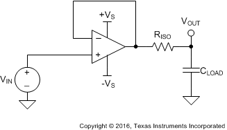 Figure 30. Unity-Gain Buffer With RISO Stability Compensation
8.2.1 Design Requirements
The design requirements are:
- Supply voltage: 30 V (±15 V)
- Capacitive loads: 100 pF, 1000 pF, 0.01 μF, 0.1 μF, and 1 μF
- Phase margin: 45° and 60°
8.2.2 Detailed Design Procedure
Figure 30 shows a unity-gain buffer driving a capacitive load. Equation 1 shows the transfer function for the circuit in Figure 30. Not shown in Figure 30 is the open-loop output resistance of the operational amplifier, RO.

The transfer function in Equation 1 has a pole and a zero. The frequency of the pole (fp) is determined by (RO + RISO) and CLOAD. Components RISO and CLOAD determine the frequency of the zero (fz). A stable system is obtained by selecting RISO such that the rate of closure (ROC) between the open-loop gain (AOL) and 1/β is 20 dB/decade. Figure 31 illustrates this concept. The 1/β curve for a unity-gain buffer is 0 dB.
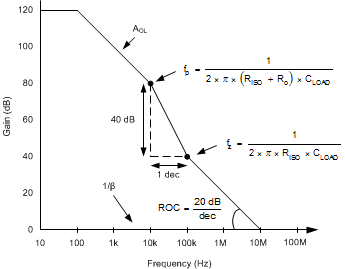 Figure 31. Unity-Gain Amplifier With RISO Compensation
ROC stability analysis is typically simulated. The validity of the analysis depends on multiple factors, especially the accurate modeling of RO. In addition to simulating the ROC, a robust stability analysis includes a measurement of overshoot percentage and ac gain peaking of the circuit using a function generator, oscilloscope, and gain and phase analyzer. Phase margin is then calculated from these measurements. Table 2 shows the overshoot percentage and ac gain peaking that correspond to phase margins of 45° and 60°. For more details on this design and other alternative devices that can be used in place of the TLV171, see the Precision Design, Capacitive Load Drive Solution Using an Isolation Resistor.
Table 2. Phase Margin versus Overshoot and AC Gain Peaking
| PHASE MARGIN | OVERSHOOT | AC GAIN PEAKING |
|---|---|---|
| 45° | 23.3% | 2.35 dB |
| 60° | 8.8% | 0.28 dB |
8.2.3 Application Curve
Using the described methodology, the values of RISO that yield phase margins of 45º and 60º for various capacitive loads were determined. The results are shown in Figure 32.
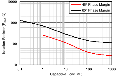 Figure 32. Isolation Resistor Required for Various Capacitive Loads to Achieve a Target Phase Margin
9 Power Supply Recommendations
The TLVx171 is specified for operation from 2.7 V to 36 V (±1.35 V to ±18 V); many specifications apply from –40°C to +85°C. Parameters that can exhibit significant variance with regard to operating voltage or temperature are presented in the Typical Characteristics section.
CAUTION
Supply voltages larger than 40 V can permanently damage the device; see the Absolute Maximum Ratings table.
Place 0.1-μF bypass capacitors close to the power-supply pins to reduce errors coupling in from noisy or high-impedance power supplies. For more detailed information on bypass capacitor placement, see the Layout section.
10 Layout
10.1 Layout Guidelines
For best operational performance of the device, use good printed-circuit board (PCB) layout practices, including:
- Noise can propagate into analog circuitry through the power pins of the circuit as a whole and the operational amplifier itself. Bypass capacitors are used to reduce the coupled noise by providing low-impedance power sources local to the analog circuitry.
- Connect low-ESR, 0.1-µF ceramic bypass capacitors between each supply pin and ground, placed as close to the device as possible. A single bypass capacitor from V+ to ground is applicable for single-supply applications.
- Separate grounding for analog and digital portions of circuitry is one of the simplest and most-effective methods of noise suppression. One or more layers on multilayer PCBs are usually devoted to ground planes. A ground plane helps distribute heat and reduces EMI noise pickup. Make sure to physically separate digital and analog grounds, paying attention to the flow of the ground current.
- In order to reduce parasitic coupling, run the input traces as far away from the supply or output traces as possible. If these traces cannot be kept separate, crossing the sensitive trace perpendicularly is much better than in parallel with the noisy trace.
- Place the external components as close to the device as possible. As illustrated in Figure 34, keeping RF and RG close to the inverting input minimizes parasitic capacitance.
- Keep the length of input traces as short as possible. Always remember that the input traces are the most sensitive part of the circuit.
- Consider a driven, low-impedance guard ring around the critical traces. A guard ring can significantly reduce leakage currents from nearby traces that are at different potentials.
10.2 Layout Example
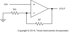 Figure 33. Schematic Representation
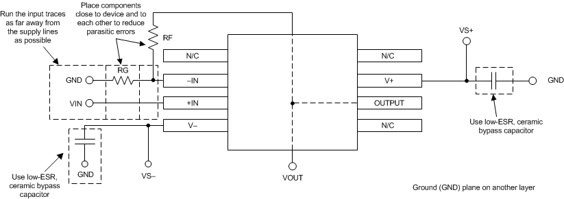 Figure 34. Operational Amplifier Board Layout for a Noninverting Configuration
11 Device and Documentation Support
11.1 Device Support
11.1.1 Development Support
11.1.1.1 TINA-TI™ (Free Software Download)
TINA™ is a simple, powerful, and easy-to-use circuit simulation program based on a SPICE engine. TINA-TI™ is a free, fully-functional version of the TINA software, preloaded with a library of macromodels in addition to a range of both passive and active models. TINA-TI™ provides all the conventional dc, transient, and frequency domain analysis of SPICE, as well as additional design capabilities.
Available as a free download from the Analog eLab Design Center, TINA-TI™ offers extensive post-processing capability that allows users to format results in a variety of ways. Virtual instruments offer the ability to select input waveforms and probe circuit nodes, voltages, and waveforms, thus creating a dynamic quick-start tool.
NOTE
These files require that either the TINA software (from DesignSoft™) or the TINA-TI™ software be installed. Download the free TINA-TI™ software from the TINA-TI™ folder.
11.1.1.2 DIP Adapter EVM
The DIP Adapter EVM tool provides an easy, low-cost way to prototype small surface-mount devices. The evaluation tool these TI packages: D or U (SOIC-8), PW (TSSOP-8), DGK (VSSOP-8), DBV (SOT23-6, SOT23-5, and SOT23-3), DCK (SC70-6 and SC70-5), and DRL (SOT563-6). The DIP adapter EVM can also be used with terminal strips or can be wired directly to existing circuits.
11.1.1.3 Universal Op Amp EVM
The Universal Op Amp EVM is a series of general-purpose, blank circuit boards that simplify prototyping circuits for a variety of device package types. The evaluation module board design allows many different circuits to be constructed easily and quickly. Five models are offered, with each model intended for a specific package type. PDIP, SOIC, MSOP, TSSOP, and SOT23 packages are all supported.
NOTE
These boards are unpopulated, so users must provide their own devices. TI recommends requesting several op amp device samples when ordering the Universal Op Amp EVM.
11.1.1.4 TI Precision Designs
TI precision designs are analog solutions created by TI’s precision analog applications experts and offer the theory of operation, component selection, simulation, a complete PCB schematic and layout, bill of materials, and measured performance of many useful circuits. TI precision designs are available online at http://www.ti.com/ww/en/analog/precision-designs/.
11.1.1.5 WEBENCH® Filter Designer
The WEBENCH® Filter Designer is a simple, powerful, and easy-to-use active filter design program. The WEBENCH® filter designer enables optimized filter designs to be created by using a selection of TI operational amplifiers and passive components from TI's vendor partners.
Available as a web-based tool from the WEBENCH® design center, the WEBENCH® filter designer allows complete multistage active filter solutions to be designed, optimized, and simulated within minutes.
11.2 Documentation Support
11.2.1 Related Documentation
For related documentation see the following:
Feedback Plots Define Op Amp AC Performance Application Bulletin (SBOA015)
11.3 Related Links
Table 3 lists quick access links. Categories include technical documents, support and community resources, tools and software, and quick access to sample or buy.
Table 3. Related Links
| PARTS | PRODUCT FOLDER | SAMPLE & BUY | TECHNICAL DOCUMENTS | TOOLS & SOFTWARE | SUPPORT & COMMUNITY |
|---|---|---|---|---|---|
| TLV171 | Click here | Click here | Click here | Click here | Click here |
| TLV2171 | Click here | Click here | Click here | Click here | Click here |
| TLV4171 | Click here | Click here | Click here | Click here | Click here |
11.4 Receiving Notification of Documentation Updates
To receive notification of documentation updates, navigate to the device product folder on ti.com. In the upper right corner, click on Alert me to register and receive a weekly digest of any product information that has changed. For change details, review the revision history included in any revised document.
11.5 Community Resources
The following links connect to TI community resources. Linked contents are provided "AS IS" by the respective contributors. They do not constitute TI specifications and do not necessarily reflect TI's views; see TI's Terms of Use.
-
TI E2E™ Online Community TI's Engineer-to-Engineer (E2E) Community. Created to foster collaboration among engineers. At e2e.ti.com, you can ask questions, share knowledge, explore ideas and help solve problems with fellow engineers.
-
Design Support TI's Design Support Quickly find helpful E2E forums along with design support tools and contact information for technical support.
11.6 Trademarks
TINA-TI, E2E are trademarks of Texas Instruments.
WEBENCH is a registered trademark of Texas Instruments.
TINA, DesignSoft are trademarks of DesignSoft, Inc.
All other trademarks are the property of their respective owners.
11.7 Electrostatic Discharge Caution

These devices have limited built-in ESD protection. The leads should be shorted together or the device placed in conductive foam during storage or handling to prevent electrostatic damage to the MOS gates.
11.8 Glossary
SLYZ022 — TI Glossary.
This glossary lists and explains terms, acronyms, and definitions.