-
TLV717P 150-mA, Low-Dropout Regulator With Foldback Current Limit for Portable Devices
- 1 Features
- 2 Applications
- 3 Description
- 4 Revision History
- 5 Pin Configuration and Functions
- 6 Specifications
- 7 Detailed Description
- 8 Application and Implementation
- 9 Power Supply Recommendations
- 10Layout
- 11Device and Documentation Support
- 12Mechanical, Packaging, and Orderable Information
- IMPORTANT NOTICE
Package Options
Mechanical Data (Package|Pins)
- DQN|4
Thermal pad, mechanical data (Package|Pins)
- DQN|4
Orderable Information
TLV717P 150-mA, Low-Dropout Regulator With Foldback Current Limit for Portable Devices
1 Features
See the Package Option Addendum at the end of this document for a complete list of available voltage options.See2 Applications
3 Description
The TLV717P series of low-dropout (LDO) linear regulators are low quiescent current LDOs with excellent line and load transient performance and are designed for power-sensitive applications. These devices provide a typical accuracy of 0.5%.
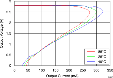
The TLV717P series offer current foldback that throttles down the output current with a decrease in load resistance. The typical value at which current foldback initiates is 350 mA; the typical value of the output short current limit value is 40 mA.
Furthermore, these devices are stable with an effective output capacitance of only 0.1 µF. This feature enables the use of cost-effective capacitors that have higher bias voltages and temperature derating. The devices regulate to specified accuracy with no output load.
The TLV717P series is available in a 1-mm × 1-mm DQN package that makes them ideal for hand-held applications. The TLV717P provides an active pulldown circuit to quickly discharge output loads.
Device Information(1)
| PART NUMBER | PACKAGE | BODY SIZE (NOM) |
|---|---|---|
| TLV717P | X2SON (4) | 1.00 mm × 1.00 mm |
- For all available packages, see the orderable addendum at the end of the data sheet.
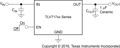
Typical Application Circuit
4 Revision History
Changes from A Revision (February 2012) to B Revision
- Deleted all instances of TLV717xx; Replaced with generic part number, TLV717PGo
- Updated Applications. Go
- Added ESD Ratings table, Feature Description section, Device Functional Modes, Application and Implementation section, Power Supply Recommendations section, Layout section, Device and Documentation Support section, and Mechanical, Packaging, and Orderable Information section Go
- Changed TJ = –25°C to TJ = 25°C in the conditions statement in Absolute Maximum RatingsGo
- Changed TA to TJ throughout Electrical CharacteristicsGo
- Changed TA to TJ in the conditions statement in Typical Characterisitcs Go
- Changed junction temperature range from –40°C to 125°C to –40°C to 85°C in OverviewGo
- Deleted TLV717xx functional block diagramGo
Changes from * Revision (October 2011) to A Revision
- Changed document status from Product Preview to Production DataGo
5 Pin Configuration and Functions


Pin Functions
| PIN | I/O | DESCRIPTION | |
|---|---|---|---|
| NAME | NO. | ||
| EN | 3 | I | Enable pin. Driving EN over 1.2 V turns on the regulator. Driving EN below 0.4 V puts the regulator into shutdown mode. |
| GND | 2 | — | Ground pin |
| IN | 4 | I | Input pin. A small capacitor is recommended from this pin to ground to assure stability. See the Input and Output Capacitor Requirements section in the Application and Implementation for more details. |
| OUT | 1 | O | Regulated output voltage pin. A small 1-μF ceramic capacitor is recommended from this pin to ground to assure stability. See the Input and Output Capacitor Requirements section in the Application and Implementation for more details. |
| Thermal pad | — | — | Connect to GND for improved thermal performance. |
6 Specifications
6.1 Absolute Maximum Ratings
At TJ = 25°C, unless otherwise noted. All voltages are with respect to GND.(1)| MIN | MAX | UNIT | ||
|---|---|---|---|---|
| Voltage | Input range, VIN | –0.3 | 6 | V |
| Enable range, VEN | –0.3 | VIN + 0.3 | ||
| Output range, VOUT | –0.3 | 6 | ||
| Current | Maximum output, IOUT | Internally limited | ||
| Output short-circuit duration | Indefinite | |||
| Continuous total power dissipation, PDISS | See Thermal Information | |||
| Temperature | Junction, TJ | –55 | 150 | °C |
| Storage junction, Tstg | –55 | 150 | ||
6.2 ESD Ratings
| VALUE | UNIT | |||
|---|---|---|---|---|
| V(ESD) | Electrostatic discharge | Human-body model (HBM), per ANSI/ESDA/JEDEC JS-001(1) | ±2000 | V |
| Charged-device model (CDM), per JEDEC specification JESD22-C101(2) | ±500 | |||
6.3 Recommended Operating Conditions
over operating junction temperature range (unless otherwise noted)| MIN | MAX | UNIT | ||
|---|---|---|---|---|
| VIN | Input voltage | 1.7 | 5.5 | V |
| VOUT | Output voltage | 1.2 | 5 | V |
| IOUT | Output current | 0 | 150 | mA |
| VEN | Enable pin voltage | 0 | VIN | V |
| TJ | Junction temperature | –40 | 85 | °C |
6.4 Thermal Information
| THERMAL METRIC | TLV717P | UNIT | |
|---|---|---|---|
| DQN (X2SON) | |||
| 4 PINS | |||
| RθJA | Junction-to-ambient thermal resistance | 393.3 | °C/W |
| RθJC(top) | Junction-to-case(top) thermal resistance | 140.3 | °C/W |
| RθJB | Junction-to-board thermal resistance | 330 | °C/W |
| ψJT | Junction-to-top characterization parameter | 6.5 | °C/W |
| ψJB | Junction-to-board characterization parameter | 329 | °C/W |
| RθJC(bot) | Junction-to-case(bottom) thermal resistance | 147.5 | °C/W |
6.5 Electrical Characteristics
At operating temperature range (TJ = –40°C to 85°C), TJ = 25°C, VIN = VOUT(NOM) + 0.5 V or 1.7 V (whichever is greater), IOUT = 10 mA, VEN = VIN, and COUT = 1 µF, unless otherwise noted.6.6 Typical Characteristics
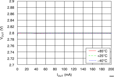
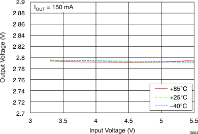
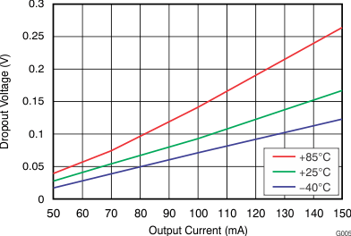
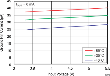
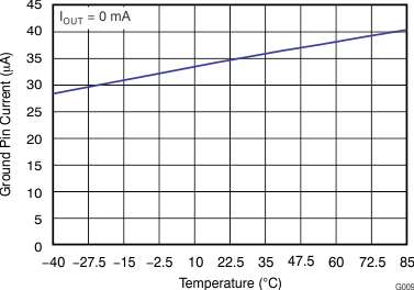
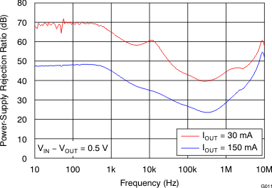
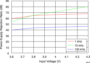
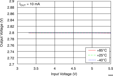
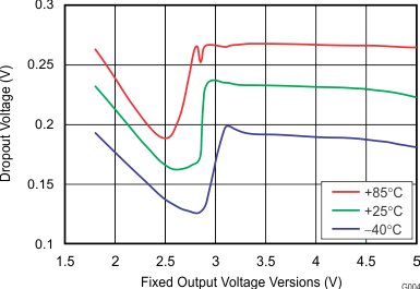
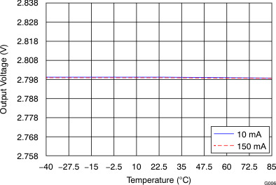
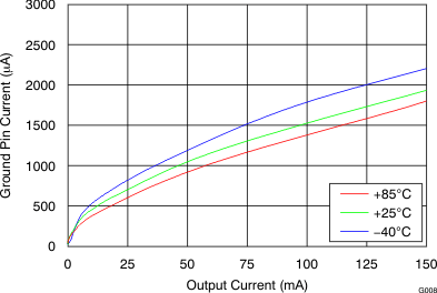
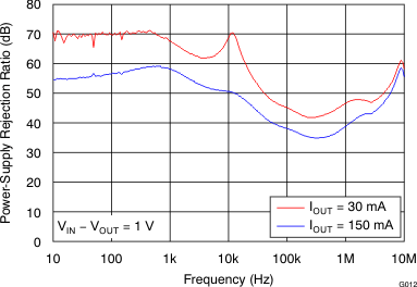
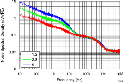
At operating temperature range (TJ = –40°C to 85°C), TJ = 25°C, VIN = VOUT(NOM) + 0.5 V or 1.7 V (whichever is greater), IOUT = 10 mA, VEN = VIN, and COUT = 1 µF, unless otherwise noted.