-
TLV936x-Q1 Automotive, 10MHz, 40V, Rail-to-Rail Output, Operational Amplifier for Cost-Sensitive Systems SBOSAD6B April 2023 – August 2024 TLV9361-Q1 , TLV9362-Q1 , TLV9364-Q1
PRODUCTION DATA
-
TLV936x-Q1 Automotive, 10MHz, 40V, Rail-to-Rail Output, Operational Amplifier for Cost-Sensitive Systems
- 1
- 1 Features
- 2 Applications
- 3 Description
- 4 Pin Configuration and Functions
- 5 Specifications
- 6 Detailed Description
- 7 Application and Implementation
- 8 Device and Documentation Support
- 9 Revision History
- 10Mechanical, Packaging, and Orderable Information
- IMPORTANT NOTICE
Package Options
Mechanical Data (Package|Pins)
Thermal pad, mechanical data (Package|Pins)
Orderable Information
TLV936x-Q1 Automotive, 10MHz, 40V, Rail-to-Rail Output, Operational Amplifier for Cost-Sensitive Systems
1 Features
- AEC-Q100 qualified for automotive applications
- Temperature grade 1: –40°C to +125°C
- Human-body model (HBM) Electrostatic discharge (ESD) classification level: 2A
- Charged-device model (CDM) ESD classification level: C6
- Low offset voltage: ±400µV
- Low offset voltage drift: ±1.25µV/°C
- Low noise: 8.5nV/√Hz at 1kHz, 6nV/√Hz broadband
- High common-mode rejection: 110dB
- Low bias current: ±10pA
- Rail-to-rail output
- Wide bandwidth: 10.6MHz GBW, unity-gain stable
- High slew rate: 25V/µs
- Low quiescent current: 2.6mA per amplifier
- Wide supply: ±2.25V to ±20V, 4.5V to 40V
- Robust EMIRR performance
3 Description
The TLV936x-Q1 family (TLV9361-Q1, TLV9362-Q1, and TLV9364-Q1) is a family of AEC-Q100 automotive qualified, 40V cost-optimized operational amplifiers.
These devices offer strong DC and AC specifications, including rail-to-rail output, low input voltage noise density (6 nV/√Hz), low offset (±400µV, typical), low offset drift (±1.25µV/°C, typical), and 10.6MHz bandwidth.
Features such as EMIRR filtering, high output current (±60mA), and high slew rate (25V/µs) make the TLV936x-Q1 a robust operational amplifier for high-voltage, cost-sensitive applications.
The TLV936x-Q1 family of op amps is available in standard packages and is specified from –40°C to 125°C.
| PART NUMBER(1) | PACKAGE | PACKAGE SIZE(2) |
|---|---|---|
| TLV9361-Q1 | DBV (SOT-23, 5) | 2.9mm × 2.8mm |
| DCK (SC70, 5) | 2mm × 2.1mm | |
| TLV9362-Q1 | D (SOIC, 8) | 4.9mm × 6mm |
| DGK (VSSOP, 8) | 3mm × 4.9mm | |
| PW (TSSOP, 8) | 3mm × 6.4mm | |
| TLV9364-Q1 | D (SOIC, 14) | 8.65mm × 6mm |
| PW (TSSOP, 14) | 5mm × 6.4mm |
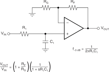 TLV936x-Q1 in a
Single-Pole, Low-Pass Filter
TLV936x-Q1 in a
Single-Pole, Low-Pass Filter4 Pin Configuration and Functions
 Figure 4-1 TLV9361-Q1 DBV Package
5-Pin SOT-23
(Top View)
 Figure 4-2 TLV9361-Q1 DCK Package
5-Pin SC70
(Top View)
| PIN | TYPE(1) | DESCRIPTION | ||
|---|---|---|---|---|
| NAME | SOT-23 | SC70 | ||
| IN+ | 3 | 1 | I | Non-inverting input |
| IN– | 4 | 3 | I | Inverting input |
| OUT | 1 | 4 | O | Output |
| V+ | 5 | 5 | — | Positive (highest) power supply |
| V– | 2 | 2 | — | Negative (lowest) power supply |
 Figure 4-3 TLV9362-Q1 D,
DGK, and PW Package
Figure 4-3 TLV9362-Q1 D,
DGK, and PW Package8-Pin SOIC, VSSOP, and TSSOP
(Top View)
| PIN | TYPE(1) | DESCRIPTION | |
|---|---|---|---|
| NAME | NO. | ||
| IN1+ | 3 | I | Non-inverting input, channel 1 |
| IN1– | 2 | I | Inverting input, channel 1 |
| IN2+ | 5 | I | Non-inverting input, channel 2 |
| IN2– | 6 | I | Inverting input, channel 2 |
| OUT1 | 1 | O | Output, channel 1 |
| OUT2 | 7 | O | Output, channel 2 |
| V+ | 8 | — | Positive (highest) power supply |
| V– | 4 | — | Negative (lowest) power supply |
 Figure 4-4 TLV9364-Q1 D and
PW Package,
Figure 4-4 TLV9364-Q1 D and
PW Package,SOIC and TSSOP
(Top View)
| PIN | TYPE(1) | DESCRIPTION | |||
|---|---|---|---|---|---|
| NAME | NO. | ||||
| IN1+ | 3 | I | Non-inverting input, channel 1 | ||
| IN1– | 2 | I | Inverting input, channel 1 | ||
| IN2+ | 5 | I | Non-inverting input, channel 2 | ||
| IN2– | 6 | I | Inverting input, channel 2 | ||
| IN3+ | 10 | I | Non-inverting input, channel 3 | ||
| IN3– | 9 | I | Inverting input, channel 3 | ||
| IN4+ | 12 | I | Non-inverting input, channel 4 | ||
| IN4– | 13 | I | Inverting input, channel 4 | ||
| OUT1 | 1 | O | Output, channel 1 | ||
| OUT2 | 7 | O | Output, channel 2 | ||
| OUT3 | 8 | O | Output, channel 3 | ||
| OUT4 | 14 | O | Output, channel 4 | ||
| V+ | 4 | — | Positive (highest) power supply | ||
| V– | 11 | — | Negative (lowest) power supply | ||
5 Specifications
5.1 Absolute Maximum Ratings
| MIN | MAX | UNIT | ||
|---|---|---|---|---|
| Supply voltage, VS = (V+) – (V–) | 0 | 42 | V | |
| Signal input pins | Common-mode voltage(3) | (V–) – 0.5 | (V+) + 0.5 | V |
| Differential voltage(3) | VS + 0.2 | V | ||
| Current(3) | –10 | 10 | mA | |
| Output short-circuit(2) | Continuous | |||
| Operating ambient temperature, TA | –55 | 150 | °C | |
| Junction temperature, TJ | 150 | °C | ||
| Storage temperature, Tstg | –65 | 150 | °C | |
5.2 ESD Ratings
| VALUE | UNIT | ||||
|---|---|---|---|---|---|
| TLV9361-Q1 | |||||
| V(ESD) | Electrostatic discharge | Human-body model (HBM), per ANSI/ESDA/JEDEC JS-001(1) | ±2000 | V | |
| Charged-device model (CDM), per ANSI/ESDA/JEDEC JS-002(2) | ±1500 | ||||
| TLV9362-Q1 and TLV9364-Q1 | |||||
| V(ESD) | Electrostatic discharge | Human-body model (HBM), per ANSI/ESDA/JEDEC JS-001(1) | ±2500 | V | |
| Charged-device model (CDM), per ANSI/ESDA/JEDEC JS-002(2) | ±1500 | ||||
5.3 Recommended Operating Conditions
| MIN | MAX | UNIT | ||
|---|---|---|---|---|
| VS | Supply voltage, (V+) – (V–) | 4.5 | 40 | V |
| VI | Common mode voltage range | (V–) | (V+) – 2 | V |
| TA | Specified temperature | –40 | 125 | °C |
5.4 Thermal Information for Single Channel
| THERMAL METRIC(1) | TLV9361-Q1 | UNIT | ||
|---|---|---|---|---|
| DBV (SOT-23) |
DCK (SC70) |
|||
| 5 PINS | 5 PINS | |||
| RθJA | Junction-to-ambient thermal resistance | 189.3 | 202.4 | °C/W |
| RθJC(top) | Junction-to-case (top) thermal resistance | 86.8 | 111.6 | °C/W |
| RθJB | Junction-to-board thermal resistance | 55.9 | 51.6 | °C/W |
| ψJT | Junction-to-top characterization parameter | 23.6 | 25.8 | °C/W |
| ψJB | Junction-to-board characterization parameter | 55.5 | 51.4 | °C/W |
| RθJC(bot) | Junction-to-case (bottom) thermal resistance | N/A | N/A | °C/W |
5.5 Thermal Information for Dual Channel
| THERMAL METRIC(1) | TLV9362-Q1 | Unit | |||
|---|---|---|---|---|---|
| D (SOIC) |
DGK (VSSOP) |
PW (TSSOP) |
|||
| 8 PINS | 8 PINS | 8 PINS | |||
| RθJA | Junction-to-ambient thermal resistance | 130.8 | 173.9 | 159.1 | °C/W |
| RθJC(top) | Junction-to-case (top) thermal resistance | 74.0 | 65.7 | 67.9 | °C/W |
| RθJB | Junction-to-board thermal resistance | 74.3 | 95.6 | 98.1 | °C/W |
| ψJT | Junction-to-top characterization parameter | 25.8 | 10.9 | 9.1 | °C/W |
| ψJB | Junction-to-board characterization parameter | 73.5 | 94.1 | 96.7 | °C/W |
| RθJC(bot) | Junction-to-case (bottom) thermal resistance | N/A | N/A | N/A | °C/W |
5.6 Thermal Information for Quad Channel
| THERMAL METRIC(1) | TLV9364-Q1 | UNIT | ||
|---|---|---|---|---|
| D (SOIC) |
PW (TSSOP) |
|||
| 14 PINS | 14 PINS | |||
| RθJA | Junction-to-ambient thermal resistance | 94.9 | 120.0 | °C/W |
| RθJC(top) | Junction-to-case (top) thermal resistance | 51.1 | 50.4 | °C/W |
| RθJB | Junction-to-board thermal resistance | 51.4 | 63.1 | °C/W |
| ψJT | Junction-to-top characterization parameter | 15.3 | 8.1 | °C/W |
| ψJB | Junction-to-board characterization parameter | 51.0 | 62.5 | °C/W |
| RθJC(bot) | Junction-to-case (bottom) thermal resistance | N/A | N/A | °C/W |
5.7 Electrical Characteristics
| PARAMETER | TEST CONDITIONS | MIN | TYP | MAX | UNIT | ||
|---|---|---|---|---|---|---|---|
| OFFSET VOLTAGE | |||||||
| VOS | Input offset voltage | VCM = V– | ±0.4 | ±1.7 | mV | ||
| TA = –40°C to 125°C | ±2 | ||||||
| dVOS/dT | Input offset voltage drift | VCM = V– | TA = –40°C to 125°C | ±1.25 | µV/℃ | ||
| PSRR | Input offset voltage versus power supply | VCM = V–, VS = 5 V to 40 V(1) | TA = –40°C to 125°C | ±1.5 | ±7.5 | μV/V | |
| DC channel separation | 1 | µV/V | |||||
| INPUT BIAS CURRENT | |||||||
| IB | Input bias current | ±10 | pA | ||||
| IOS | Input offset current | ±10 | pA | ||||
| NOISE | |||||||
| EN | Input voltage noise | f = 0.1 Hz to 10 Hz | 6 | μVPP | |||
| 1 | µVRMS | ||||||
| eN | Input voltage noise density | f = 1 kHz | 8.5 | nV/√Hz | |||
| f = 10 kHz | 6 | ||||||
| iN | Input current noise density | f = 1 kHz | 100 | fA/√Hz | |||
| INPUT VOLTAGE RANGE | |||||||
| VCM | Common-mode voltage range | (V–) | (V+) – 2 | V | |||
| CMRR | Common-mode rejection ratio | VS = 40 V, V– < VCM < (V+) – 2 V | TA = –40°C to 125°C | 95 | 110 | dB | |
| VS = 5 V, V– < VCM < (V+) – 2 V(1) | 75 | 85 | |||||
| INPUT IMPEDANCE | |||||||
| ZID | Differential | 100 || 9 | MΩ || pF | ||||
| ZICM | Common-mode | 6 || 1 | TΩ || pF | ||||
| OPEN-LOOP GAIN | |||||||
| AOL | Open-loop voltage gain | VS = 40 V, VCM = VS / 2, (V–) + 0.1 V < VO < (V+) – 0.1 V |
115 | 130 | dB | ||
| VS = 40 V, VCM = VS / 2, (V–) + 0.12 V < VO < (V+) – 0.12 V |
TA = –40°C to 125°C | 130 | |||||
| VS = 5 V, VCM = VS / 2, (V–) + 0.1 V < VO < (V+) – 0.1 V(1) |
100 | 120 | |||||
| TA = –40°C to 125°C | 120 | ||||||
| FREQUENCY RESPONSE | |||||||
| GBW | Gain-bandwidth product | 10.6 | MHz | ||||
| SR | Slew rate | VS = 40 V, G = +1, VSTEP = 10 V, CL = 20 pF(3) | 25 | V/μs | |||
| tS | Settling time | To 0.1%, VS = 40 V, VSTEP = 10 V, G = +1, CL = 20 pF | 0.65 | μs | |||
| To 0.1%, VS = 40 V, VSTEP = 2 V, G = +1, CL = 20 pF | 0.3 | ||||||
| To 0.01%, VS = 40 V, VSTEP = 10 V, G = +1, CL = 20 pF | 0.86 | ||||||
| To 0.01%, VS = 40 V, VSTEP = 2 V, G = +1, CL = 20 pF | 0.44 | ||||||
| Phase margin | G = +1, RL = 10 kΩ, CL = 20 pF | 64 | ° | ||||
| Overload recovery time | VIN × gain > VS | 170 | ns | ||||
| THD+N | Total harmonic distortion + noise | VS = 40 V, VO = 3 VRMS, G = 1, f = 1 kHz, RL = 10 kΩ | 0.0001% | ||||
| 120 | dB | ||||||
| VS = 10 V, VO = 3 VRMS, G = 1, f = 1 kHz, RL = 128 Ω | 0.0056% | ||||||
| 85 | dB | ||||||
| VS = 10 V, VO = 0.4 VRMS, G = 1, f = 1 kHz, RL = 32 Ω | 0.00056% | ||||||
| 105 | dB | ||||||
| OUTPUT | |||||||
| Voltage output swing from rail | Positive and negative rail headroom |
VS = 40 V, RL = no load | 10 | mV | |||
| VS = 40 V, RL = 10 kΩ | 60 | 100 | |||||
| VS = 40 V, RL = 2 kΩ | 250 | 400 | |||||
| ISC | Short-circuit current | ±60(2) | mA | ||||
| CLOAD | Capacitive Load Drive | See Figure 5-28 | pF | ||||
| ZO | Open-loop output impedance | IO = 0 A | See Figure 5-25 | Ω | |||
| POWER SUPPLY | |||||||
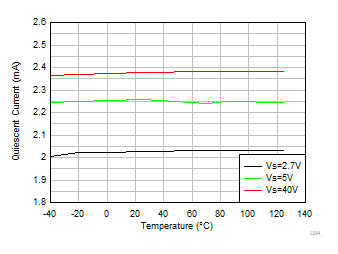
| IQ | Quiescent current per amplifier | IO = 0 A | 2.6 | 3 | mA | ||
| TA = –40°C to 125°C | 3.2 | ||||||
5.8 Typical Characteristics
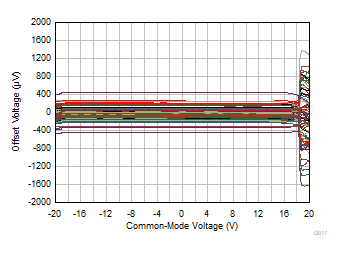
at TA = 25°C, VS = ±20V, VCM = VS / 2, RLOAD = 10kΩ (unless otherwise noted)
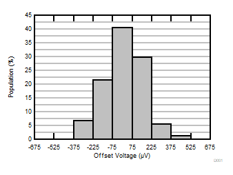
| Distribution from 74 amplifiers, TA = 25°C |
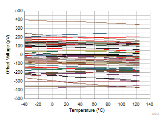
| VCM = V- | ||
| Data from 74 amplifiers |
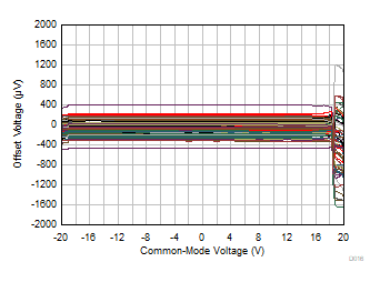
| TA = 125°C | ||
| Data from 74 amplifiers |
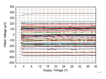
| VCM = V– | ||
| Data from 74 amplifiers |
 Figure 5-9 Input
Bias Current and Offset Current vs Common-Mode Voltage
| G = +1, CL = 20 pF |

| VS = 40V |
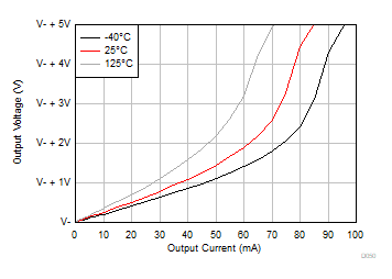
| VS = 5V |
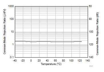
| VS = 40V |
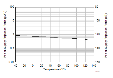
 Figure 5-21 Input
Voltage Noise Spectral Density vs Frequency
| VCM = V– |
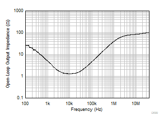 Figure 5-25 Open-Loop Output Impedance vs Frequency
| 20mVpp Output Step, G = +1 |

| G = –10 |
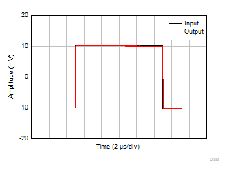
| CL = 20pF, G = 1, 20mVpp step response |
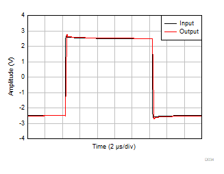
| CL = 20pF, G = 1, 5Vpp step response |
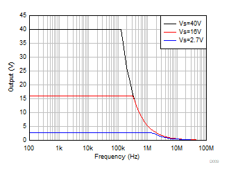 Figure 5-35 Maximum Output Voltage vs Frequency
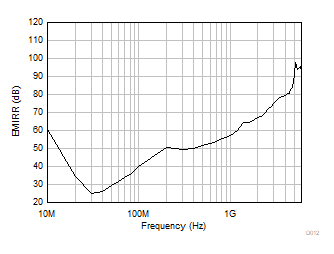 Figure 5-37 EMIRR
(Electromagnetic Interference Rejection Ratio) vs Frequency
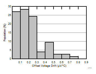
| Distribution from 74 amplifiers |
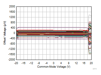
| TA = 25°C | ||
| Data from 74 amplifiers |
| TA = –40°C | ||
| Data from 74 amplifiers |
 Figure 5-8 Closed-Loop Gain vs Frequency
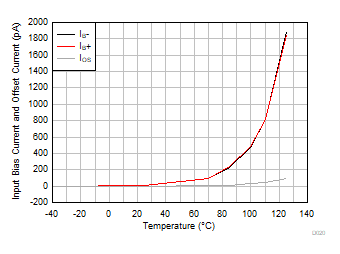 Figure 5-10 Input
Bias Current and Offset Current vs Temperature
| VS = 40 V |

| VS = 5V |

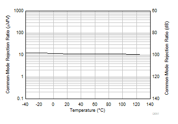
| VS = 5V |
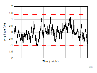 Figure 5-20 0.1Hz to 10-Hz
Noise
| VCM = V– |
 Figure 5-24 Open-Loop Voltage Gain vs Temperature (dB)
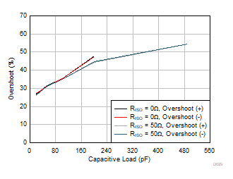
| 20mVpp Output Step, G = -1 |

| G = +1 |
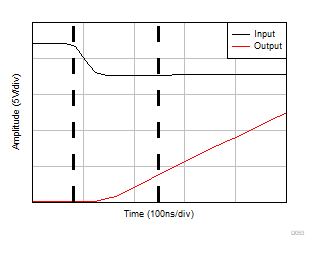
| G = –10 |
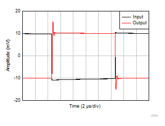
| CL = 20pF, G = -1, 20mVpp step response |
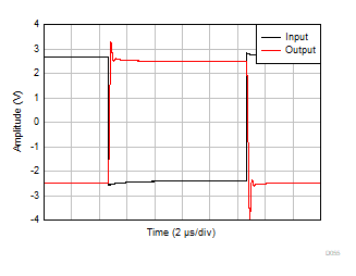
| CL = 20pF, G = -1, 5Vpp step response |
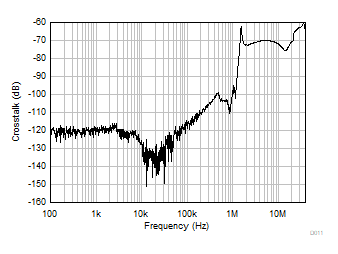 Figure 5-36 Channel Separation vs Frequency