-
TPD1E01B04-Q1 Automotive 0.2-pF, ±3.6-V, ±15-kVESD Protection Diode in 0402 Package
- 1 Features
- 2 Applications
- 3 Description
- 4 Revision History
- 5 Pin Configuration and Functions
- 6 Specifications
-
7 Detailed Description
- 7.1 Overview
- 7.2 Functional Block Diagram
- 7.3
Feature Description
- 7.3.1 IEC 61000-4-2 ESD Protection
- 7.3.2 IEC 61000-4-4 EFT Protection
- 7.3.3 IEC 61000-4-5 Surge Protection
- 7.3.4 IO Capacitance
- 7.3.5 DC Breakdown Voltage
- 7.3.6 Ultra Low Leakage Current
- 7.3.7 Low ESD Clamping Voltage
- 7.3.8 Supports High Speed Interfaces
- 7.3.9 Industrial Temperature Range
- 7.3.10 Easy Flow-Through Routing Package
- 7.4 Device Functional Modes
- 8 Application and Implementation
- 9 Power Supply Recommendations
- 10Layout
- 11Device and Documentation Support
- 12Mechanical, Packaging, and Orderable Information
- IMPORTANT NOTICE
Package Options
Mechanical Data (Package|Pins)
- DPY|2
Thermal pad, mechanical data (Package|Pins)
- DPY|2
Orderable Information
TPD1E01B04-Q1 Automotive 0.2-pF, ±3.6-V, ±15-kVESD Protection Diode in 0402 Package
1 Features
- IEC 61000-4-2 level 4 ESD protection
- ±15-kV contact discharge
- ±17-kV air gap discharge
- IEC 61000-4-4 EFT protection
- 80 A (5/50 ns)
- IEC 61000-4-5 surge protection
- 2.5 A (8/20 µs)
- IO capacitance:
- 0.20 pF (typical)
- 0.23 pF (maximum)
- DC breakdown voltage: 6.4 V (typical)
- Ultra low leakage current: 10-nA (maximum)
- Low ESD clamping voltage: 15 V at 16 A TLP
- Low insertion loss: 20 GHz
- Supports high speed interfaces up to 20 Gbps
- Industry standard 0402 footprint
- AEC-Q101
qualified
- Device HBM classification level H2
- Device CDM classification level C5
- Device operating temperature range: –40°C to +125°C
2 Applications
- End equipment
- Interfaces
- Automotive SerDes: FPD-Link
- USB Type-C
- USB 3.1 Gen 2/3.0/2.0
- HDMI 2.0/1.4
- 10/100/1000 Mbps ethernet
3 Description
The TPD1E01B04-Q1 is a bidirectional TVS ESD protection diode for USB Type-C and FPD-Link circuit protection. The TPD1E01B04-Q1 is rated to dissipate ESD strikes at the maximum level specified in the IEC 61000-4-2 international standard (Level 4).
This device features a 0.20-pF (typical) IO capacitance making it ideal for protecting high-speed interfaces up to 20 Gbps such as USB 3.1 Gen2 and FPD-Link. The low dynamic resistance and low clamping voltage ensure system level protection against transient events.
The TPD1E01B04-Q1 is offered in the industry standard 0402 (DPY) package.
| PART NUMBER | PACKAGE | BODY SIZE (NOM) |
|---|---|---|
| TPD1E01B04-Q1 | X1SON (2) | 1.00 mm x 0.60 mm |
 Typical Application
4 Revision History
Changes from Revision * (May 2021) to Revision A (December 2021)
- Changed the status of the data sheet from: Advanced Information to: Production Data Go
5 Pin Configuration and Functions
 Figure 5-1 DPY Package2-Pin X1SONTop View
| PIN | TYPE(1) | DESCRIPTION | |
|---|---|---|---|
| NO. | NAME | ||
| 1 | IO | I/O | ESD Protected Channel. If used as ESD IO, connect pin 2 to ground |
| 2 | IO | I/O | ESD Protected Channel. If used as ESD IO, connect pin 1 to ground |
6 Specifications
6.1 Absolute Maximum Ratings
| MIN | MAX | UNIT | ||
|---|---|---|---|---|
| Electrical fast transient | IEC 61000-4-5 (5/50 ns) at 25°C | 80 | A | |
| Peak pulse | IEC 61000-4-5 power (tp - 8/20 µs) at 25°C | 27 | W | |
| IEC 61000-4-5 current (tp - 8/20 µs) at 25°C | 2.5 | A | ||
| TA | Operating free-air temperature | –40 | 125 | °C |
| Tstg | Storage temperature | –65 | 155 | °C |
6.2 ESD Ratings—AEC Specification
| VALUE | UNIT | |||
|---|---|---|---|---|
| V(ESD) | Electrostatic discharge | Human body model (HBM), per AEC Q101-001 | ±2500 | V |
| Charged device model (CDM), per AEC Q101-005 | ±1000 | |||
6.3 ESD Ratings—IEC Specification
| VALUE | UNIT | |||
|---|---|---|---|---|
| V(ESD) | Electrostatic discharge | IEC 61000-4-2 Contact Discharge, all pins | ±15000 | V |
| IEC 61000-4-2 Air-gap Discharge, all pins | ±17000 | |||
6.4 ESD Ratings—ISO Specification
| VALUE | UNIT | ||||
|---|---|---|---|---|---|
| V(ESD) | Electrostatic discharge | ISO 10605, 330-pF, 330-Ω, IO | Contact discharge | ± 12500 | V |
| Air-gap discharge | ±15000 | ||||
6.5 Recommended Operating Conditions
| MIN | NOM | MAX | UNIT | ||
|---|---|---|---|---|---|
| VIO | Input pin voltage | –3.6 | 3.6 | V | |
| TA | Operating free-air temperature | –40 | 125 | °C | |
6.6 Thermal Information
| THERMAL METRIC(1) | TPD1E01B04-Q1 | UNIT | |
|---|---|---|---|
| DPY (X1SON) | |||
| 2 PINS | |||
| RθJA | Junction-to-ambient thermal resistance | 442.6 | °C/W |
| RθJC(top) | Junction-to-case (top) thermal resistance | 243.8 | °C/W |
| RθJB | Junction-to-board thermal resistance | 162.5 | °C/W |
| ΨJT | Junction-to-top characterization parameter | 154.1 | °C/W |
| ΨJB | Junction-to-board characterization parameter | 163.0 | °C/W |
| RθJC(bot) | Junction-to-case (bottom) thermal resistance | n/a | °C/W |
6.7 Electrical Characteristics
| PARAMETER | TEST CONDITIONS | MIN | TYP | MAX | UNIT | ||
|---|---|---|---|---|---|---|---|
| VRWM | Reverse stand-off voltage | IIO < 10 nA | –3.6 | 3.6 | V | ||
| VBRF | Breakdown voltage, IO pin to GND | Measured as the maximum voltage before device snaps back into VHOLD voltage | 6.4 | V | |||
| VBRR | Breakdown voltage, GND to IO pin | –6.4 | V | ||||
| VHOLD | Holding voltage | IIO = 1 mA, TA = 25°C | 5 | 5.9 | 6.5 | V | |
| VCLAMP | Clamping voltage | IPP = 1 A, TLP, from IO to GND | 7 | V | |||
| IPP = 5 A, TLP, from IO to GND | 9.2 | ||||||
| IPP = 16 A, TLP, from IO to GND | 15 | ||||||
| IPP = 1 A, TLP, from GND to IO | 7 | ||||||
| IPP = 5 A, TLP, from GND to IO | 9.2 | ||||||
| IPP = 16 A, TLP, from GND to IO | 15 | ||||||
| ILEAK | Leakage current, IO to GND | VIO = ±2.5 V | 10 | nA | |||
| RDYN | Dynamic resistance | IO to GND | 0.57 | Ω | |||
| GND to IO | 0.57 | ||||||
| CL | Line capacitance | VIO = 0 V, f = 1 MHz, IO to GND, TA = 25°C | 0.2 | 0.23 | pF | ||
6.8 Typical Characteristics
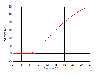 Figure 6-1 Positive TLP Curve
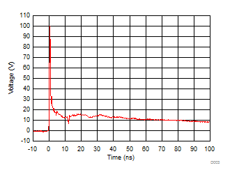 Figure 6-3 8-kV IEC Waveform
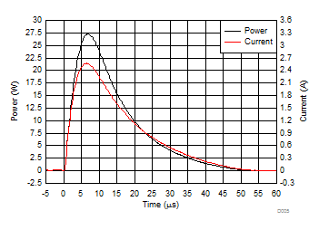 Figure 6-5 Surge Curve (tp = 8/20µs), IO pin to GND
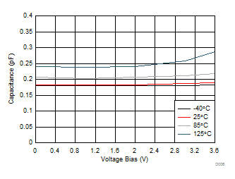 Figure 6-7 Capacitance vs. Bias Voltage (DPY Package)
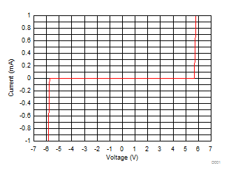 Figure 6-9 DC Voltage Sweep I-V Curve
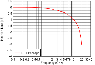 Figure 6-11 Insertion Loss
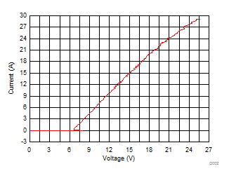 Figure 6-2 Negative TLP Curve
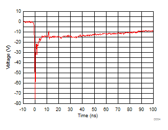 Figure 6-4 –8-kV IEC Waveform
 Figure 6-6 Capacitance vs. Bias
Voltage
 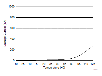 Figure 6-8 Leakage Current vs. Temperature
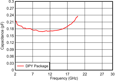 Figure 6-10 Capacitance vs. Frequency
7 Detailed Description
7.1 Overview
The TPD1E01B04-Q1 device is a bidirectional ESD Protection Diode with ultra-low capacitance. This device can dissipate ESD strikes above the maximum level specified by the IEC 61000-4-2 International Standard. The ultra-low capacitance makes this device ideal for protecting any super high-speed signal pins including Thunderbolt 3. The low capacitance allows for extremely low losses even at RF frequencies such as USB 3.1 Gen 2, Thunderbolt 3, or antenna applications.