SLLSEB2E February 2012 – October 2015 TPD1E6B06
PRODUCTION DATA.
- 1 Features
- 2 Applications
- 3 Description
- 4 Revision History
- 5 Pin Configuration and Functions
- 6 Specifications
- 7 Detailed Description
- 8 Application and Implementation
- 9 Power Supply Recommendations
- 10Layout
- 11Device and Documentation Support
- 12Mechanical, Packaging, and Orderable Information
Package Options
Mechanical Data (Package|Pins)
- DPL|2
Thermal pad, mechanical data (Package|Pins)
- DPL|2
Orderable Information
1 Features
- IEC 61000-4-2 Level 4 ESD Protection
- ±15-kV Contact Discharge
- ±15-kV Air-Gap Discharge
- IEC 61000-4-5 Surge: 3.8 A (8/20 µs)
- I/O Capacitance: 6 pF (Typical)
- RDYN: 0.55 Ω (Typical)
- DC Breakdown Voltage: ±6 V (Minimum)
- Low Leakage Current: 10 nA (Typical)
- Low ESD Clamping Voltage
- Industrial Temperature Range: –40°C to 125°C
- Space-Saving 0201 Footprint
(0.6 mm × 0.3 mm × 0.3 mm)
2 Applications
- End Equipment
- Mobile Phones
- Tablets
- Wearables
- Remote Controllers
- Electronic Point of Sale (EPOS)
- Interfaces
- Audio Lines
- General-Purpose Input/Output (GPIO)
- Pushbuttons
3 Description
The TPD1E6B06 device is a single-channel TVS diode for electrostatic discharge (ESD) protection in a small 0201 package. The TPD1E6B06 is rated to dissipate ESD strikes above the maximum level specified in the IEC 61000-4-2 international standard (Level 4), with ±15-kV contact discharge and ±15-kV air-gap ESD protection. The device has a back-to-back TVS diode configuration for bipolar or bidirectional signal support. The 6-pF line capacitance is suitable to provide transient voltage suppression circuit protection for a wide range of applications, supporting data rates up to
800 Mbps.
Typical application interfaces for the TPD1E6B06 are audio lines (microphone, earphone, and speakerphone), SD interfacing, keypad or other buttons, as well as the VBUS and ID pins of USB ports. With its industry-standard 0201 package, The TPD1E6B06 has an extremely small footprint, making it ideal for space-saving end equipment like mobile phones, tablets, and wearables.
Device Information(1)
| PART NUMBER | PACKAGE | BODY SIZE (NOM) |
|---|---|---|
| TPD1E6B06 | X2SON (2) | 0.60 mm × 0.30 mm |
- For all available packages, see the orderable addendum at the end of the data sheet.
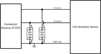
Simplified Schematic
