-
TPS22975 5.7-V, 6-A, 16-mΩ On-Resistance Load Switch
- 1 Features
- 2 Applications
- 3 Description
- 4 Revision History
- 5 Device Comparison Table
- 6 Pin Configuration and Functions
- 7 Specifications
- 8 Parameter Measurement Information
- 9 Detailed Description
- 10Application and Implementation
- 11Power Supply Recommendations
- 12Layout
- 13Device and Documentation Support
- 14Mechanical, Packaging, and Orderable Information
- IMPORTANT NOTICE
Package Options
Mechanical Data (Package|Pins)
- DSG|8
Thermal pad, mechanical data (Package|Pins)
- DSG|8
Orderable Information
TPS22975 5.7-V, 6-A, 16-mΩ On-Resistance Load Switch
1 Features
- Integrated Single-Channel Load Switch
- Input Voltage Range: 0.6 V to VBIAS
- VBIAS Voltage Range: 2.5 V to 5.7 V
- On-Resistance (RON)
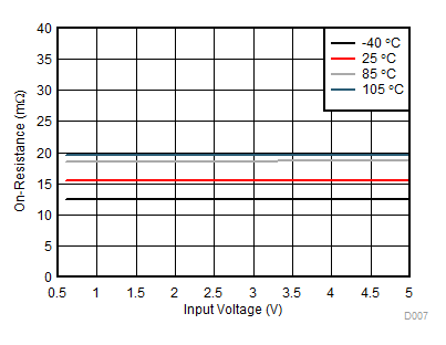
- RON = 16 mΩ (typical) at VIN = 0.6 V to 5.7 V,
VBIAS = 5.7 V
- RON = 16 mΩ (typical) at VIN = 0.6 V to 5.7 V,
- 6-A Maximum Continuous Switch Current
- Low Quiescent Current
- 37 µA (typical) at VIN = VBIAS = 5 V
- Low-Control Input-Threshold Enables Use of
1.2-, 1.8-, 2.5-, and 3.3-V Logic - Configurable Rise Time
- Thermal Shutdown
- Quick-Output Discharge (QOD) (Optional)
- SON 8-pin Package with Thermal Pad
- ESD Performance Tested per JESD 22
- 2000-V HBM and 1000-V CDM
2 Applications
- Ultrabook™
- Notebooks and Netbooks
- Tablet PC
- Consumer Electronics
- Set-top Boxes and Residential Gateways
- Telecom Systems
- Solid State Drives (SSDs)
3 Description
The TPS22975 product family consists of two devices: TPS22975 and TPS22975N. Each device is a single-channel load switch that provides a configurable rise time to minimize inrush current. The device contains an N-channel MOSFET that can operate over an input voltage range of 0.6 V to 5.7 V and can support a maximum continuous current of 6 A. The switch is controlled by an on and off input (ON), which is capable of interfacing directly with low-voltage control signals. TPS22975 has an optional 230-Ω on-chip load resistor for quick output discharge when switch is turned off.
The TPS22975 is available in a small, space-saving 2-mm × 2-mm 8-pin SON package (DSG) with integrated thermal pad allowing for high power dissipation. The device is characterized for operation over the free-air temperature range of –40°C to +105°C.
Device Information(1)
| PART NUMBER | PACKAGE | BODY SIZE (NOM) |
|---|---|---|
| TPS22975 TPS22975N |
WSON (8) | 2.00 mm × 2.00 mm |
- For all available packages, see the orderable addendum at the end of the data sheet.
Simplified Schematic

On-Resistance vs Input Voltage

4 Revision History
Changes from A Revision (June 2016) to B Revision
- Updated VIH in Recommended Operating ConditionsGo
Changes from * Revision (May 2016) to A Revision
- Changed device status from Product Preview to Production Data Go
5 Device Comparison Table
| DEVICE | RON AT VIN = VBIAS = 5 V (TYPICAL) | QUICK-OUTPUT DISCHARGE | MAXIMUM OUTPUT CURRENT | ENABLE |
|---|---|---|---|---|
| TPS22975 | 16 mΩ | Yes | 6 A | Active high |
| TPS22975N | 16 mΩ | No | 6 A | Active high |
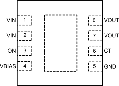
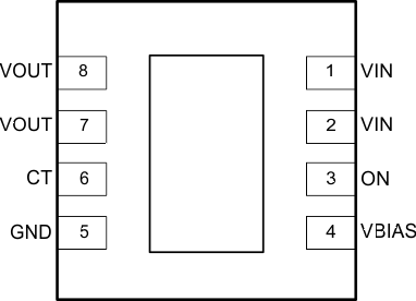
6 Pin Configuration and Functions


Pin Functions
| PIN | I/O | DESCRIPTION | |
|---|---|---|---|
| NO. | NAME | ||
| 1 | VIN | I | Switch input. Input bypass capacitor recommended for minimizing VIN dip. Must be connected to Pin 1 and Pin 2. See the Application and Implementation section for more information |
| 2 | |||
| 3 | ON | I | Active high switch control input. Do not leave floating |
| 4 | VBIAS | I | Bias voltage. Power supply to the device. Recommended voltage range for this pin is 2.5 V to 5.7 V. See the Application and Implementation section for more information |
| 5 | GND | — | Device ground |
| 6 | CT | O | Switch slew rate control. Can be left floating. See the Adjustable Rise Time section under Feature Description for more information |
| 7 | VOUT | O | Switch output |
| 8 | |||
| — | Thermal Pad | — | Thermal pad (exposed center pad) to alleviate thermal stress. Tie to GND. See the Layout Example section for layout guidelines |