-
TPS25200-Q1 5-V eFuse With Precision Adjustable Current Limit and Overvoltage Clamp
- 1 Features
- 2 Applications
- 3 Description
- 4 Simplified Schematic
- 5 Revision History
- 6 Pin Configuration and Functions
- 7 Specifications
- 8 Parameter Measurement Information
- 9 Detailed Description
- 10Application and Implementation
- 11Power Supply Recommendations
- 12Layout
- 13Device and Documentation Support
- 14Mechanical, Packaging, and Orderable Information
- IMPORTANT NOTICE
Package Options
Mechanical Data (Package|Pins)
- DRV|6
Thermal pad, mechanical data (Package|Pins)
- DRV|6
Orderable Information
TPS25200-Q1 5-V eFuse With Precision Adjustable Current Limit and Overvoltage Clamp
1 Features
- Qualified for Automotive Applications
- AEC-Q100 Qualified With the Following Results:
- Device HBM Classification Level 2
- Device CDM Classification Level C5
- 2.5-V to 6.5-V Operation
- 20-V Continuous VIN (Absolute Maximum)
- 7.6-V Input Overvoltage Shutoff
- 5.25-V to 5.55-V Fixed Overvoltge Clamp
- 0.6-μs Overvoltage Lockout Response
- 3.5-μs Short-Circuit Response
- 67-mΩ High-Side MOSFET
- Accurate 2.5-A Minimum, 2.9-A Maximum and 2.1-A Minimum, 2.5-A Maximum Setting (Including Resistor)
- ±6.3% Current-Limit Accuracy at 2.7 A
- Reverse Current Blocking While Disabled
- Built-in Soft Start
- Pin-to-Pin Compatible with TPS2553
2 Applications
- Automotive USB Port Protection
- USB Power Switch .
- USB Slave Devices
3 Description
The TPS25200-Q1 device is a 5-V eFuse with a precision current-limit and overvoltage clamp. The device provides robust protection for load and source during overvoltage and overcurrent events.
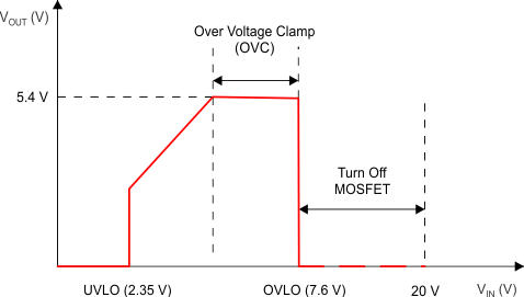
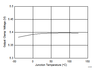
The TPS25200-Q1 device is an intelligent protected load-switch with a VIN value tolerant to 20 V. In the event that an incorrect voltage is applied at the IN pin, the output clamps to 5.4 V to protect the load. If the voltage at the IN pin exceeds 7.6 V, the device disconnects the load to prevent damage to the device, load, or both.
The TPS25200-Q1 device has an internal 67-mΩ power switch and is intended for protecting the source, device, and load under a variety of abnormal conditions. The device provides up to 2.4 A of continuous load current. The current-limit is programmable from 85 mA to 2.7 A with a single resistor to ground. During overload events, the output current is limited to the level set by the RILIM resistor. If a persistent overload occurs, the device eventually enters thermal shutoff to prevent damage to the TPS25200-Q1 device.
Device Information(1)
| PART NUMBER | PACKAGE | BODY SIZE (NOM) |
|---|---|---|
| TPS25200-Q1 | WSON (6) | 2.00 mm × 2.00 mm |
- For all available packages, see the orderable addendum at the end of the datasheet.
4 Simplified Schematic
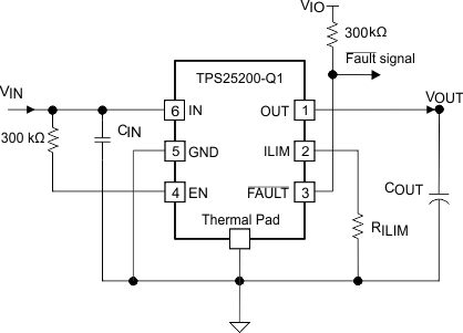
VOUT vs VIN
5 Revision History
| DATE | REVISION | NOTES |
|---|---|---|
| March 2015 | * | Initial release. |
6 Pin Configuration and Functions
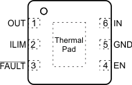
Pin Functions
| PIN | I/O | DESCRIPTION | |
|---|---|---|---|
| NAME | NO. | ||
| EN | 4 | I | Logic-level control input. When this pin is driven high, the power switch is enabled. When this pin is driven low, the power switch turns off. This pin cannot be left floating and it must be limited below the absolute maximum rating if tied to the IN pin. |
| FAULT | 3 | O | Active-low open-drain output. This pin is asserted during an overcurrent, overvoltage, or overtemperature event. Connect a pullup resistor to the logic I/O voltage. |
| GND | 5 | — | Ground connection. Connect this pin externally to the exposed thermal pad. |
| ILIM | 2 | O | External resistor. The ILIM pin is used to set the current-limit threshold. The recommended value for this pin is: 36 kΩ ≤ RILIM ≤ 1100 kΩ. |
| IN | 6 | I | Input voltage. Connect a ceramic capacitor with a value of 0.1 μF or greater from the IN pin to the GND pin as close to the IC as possible. |
| OUT | 1 | O | Protected power switch, VOUT. |
| Thermal pad | — | The exposed thermal pad is internally connected to the GND pin. Use the thermal pad to heat-sink the device to the circuit board traces. Connect the thermal pad to the GND pin externally. | |
7 Specifications
7.1 Absolute Maximum Ratings
over operating free-air temperature range, voltage are referenced to GND (unless otherwise noted)(1)| MIN | MAX | UNIT | ||
|---|---|---|---|---|
| Voltage | IN | –0.3 | 20 | V |
| OUT, EN, ILIM, FAULT | –0.3 | 7 | V | |
| From IN to OUT | –7 | 20 | V | |
| Continuous output current, IO | Thermally Limited | |||
| Continuous FAULT output sink current | 25 | mA | ||
| Continuous ILIM output source current | 150 | µA | ||
| Operating junction temperature, TJ | Internally limited | |||
| Storage temperature, Tstg | –65 | 150 | °C | |
7.2 ESD Ratings
| VALUE | UNIT | ||||
|---|---|---|---|---|---|
| V(ESD) | Electrostatic discharge | Human body model (HBM), per AEC Q100-002(1) | ±2000 | V | |
| Charged device model (CDM), per AEC Q100-011 | ±750 | ||||
7.3 Recommended Operating Conditions
over operating free-air temperature range (unless otherwise noted)| MIN | MAX | UNIT | ||
|---|---|---|---|---|
| VIN | Input voltage of IN | 2.5 | 6.5 | V |
| VEN | Enable pin voltage | 0 | 6.5 | V |
| IFAULT | Continuous FAULT sink current | 0 | 10 | mA |
| IOUT | Continuous output current of OUT | 2.4 | A | |
| RILIM | Current-limit set resistors | 36 | 1100 | kΩ |
| TJ | Operating junction temperature | –40 | 125 | °C |
7.4 Thermal Information
| THERMAL METRIC(1) | DRV (WSON) | UNIT | |
|---|---|---|---|
| 6 PINS | |||
| RθJA | Junction-to-ambient thermal resistance | 66.5 | °C/W |
| RθJC(top) | Junction-to-case (top) thermal resistance | 83.4 | |
| RθJB | Junction-to-board thermal resistance | 36.1 | |
| ψJT | Junction-to-top characterization parameter | 1.6 | |
| ψJB | Junction-to-board characterization parameter | 36.5 | |
| RθJC(bot) | Junction-to-case (bottom) thermal resistance | 7.6 | |
7.5 Electrical Characteristics
Conditions are –40°C ≤ TJ ≤ 125°C and 2.5 V ≤ VIN ≤ 6.5 V. VEN = VIN, RILIM = 36 kΩ. Positive current into pins. Typical value is at 25°C. All voltages are with respect to ground (unless otherwise noted).| PARAMETER | TEST CONDITIONS | MIN | TYP | MAX | UNIT | ||
|---|---|---|---|---|---|---|---|
| POWER SWITCH | |||||||
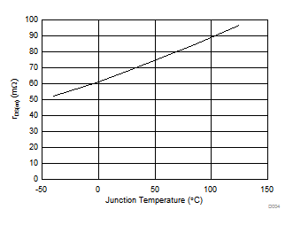
| rDS(on) | IN–OUT resistance(1) | 2.5 V ≤ VIN ≤ 5 V, IOUT = 2.4 A |
TJ = 25°C | 67 | 75 | mΩ | |
| –40°C ≤ TJ ≤ 85°C | 67 | 95 | |||||
| –40°C ≤ TJ ≤ 125°C | 67 | 105 | |||||
| ENABLE INPUT EN | |||||||
| EN pin turn on threshold | Input rising | 1.9 | V | ||||
| EN pin turn off threshold | Input falling | 0.6 | V | ||||
| Hysteresis | 330(2) | mV | |||||
| IEN | Leakage current | VEN = 0 V or 5.5 V | –2 | 2 | µA | ||
| DISCHARGE | |||||||
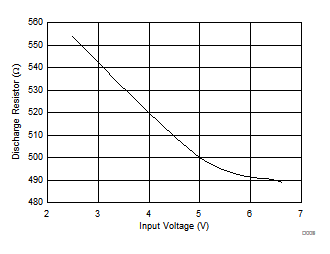
| RDCHG | OUT Discharge Resistance | VOUT = 5 V, VEN = 0 V | 500 | 625 | Ω | ||
| CURRENT LIMIT | |||||||
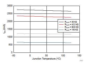
| IOS | Current-limit, see Figure 12 | RILIM = 36 kΩ | 2530 | 2700 | 2870 | mA | |
| RILIM = 42.2 kΩ | 2140 | 2300 | 2460 | ||||
| RILIM = 56 kΩ | 1620 | 1740 | 1860 | ||||
| RILIM = 80.6 kΩ | 1110 | 1206 | 1300 | ||||
| RILIM = 150 kΩ | 590 | 647 | 710 | ||||
| RILIM = 1100 kΩ | 40 | 83 | 130 | ||||
| OVERVOLTAGE LOCKOUT, IN | |||||||
| V(OVLO) | IN rising OVLO threshold voltage | IN rising | 6.8 | 7.6 | 8.45 | V | |
| Hysteresis | 70(2) | mV | |||||
| VOLTAGE CLAMP, OUT | |||||||
| V(OVC) | OUT clamp voltage threshold | CL = 1 µF, RL = 100 Ω, VIN = 6.5 V | 5.25 | 5.4 | 5.55 | V | |
| SUPPLY CURRENT | |||||||
| IIN(off) | Supply current, low-level output | VEN = 0 V, VIN = 5 V | 1 | 5 | µA | ||
| VEN = 0 or 5 V, VIN = 20 V | 1040 | 1700 | |||||
| IIN(on) | Supply current, high-level output | VIN = 5 V, No load on OUT |
RILIM = 36 kΩ | 147 | 200 | µA | |
| RILIM = 150 kΩ | 120 | 190 | |||||
| IREV | Reverse leakage current | VOUT = 6.5V, VIN = VEN = 0 V, TJ = 25°C, Measure IOUT | 3.2 | 5 | µA | ||
| UNDERVOLTAGE LOCKOUT, IN | |||||||
| VUVLO | IN rising UVLO threshold voltage | IN rising | 2.35 | 2.45 | V | ||
| Hysteresis | 30(2) | mV | |||||
| FAULT FLAG | |||||||
| VOL | Output low voltage, FAULT | IFAULT = 1 mA | 50 | 180 | mV | ||
| Off-state leakage | VFAULT = 6.5 V | 1 | µA | ||||
| THERMAL SHUTDOWN | |||||||
| Thermal shutdown threshold, OTSD2(3) | 155 | °C | |||||
| Thermal shutdown threshold only in current-limit, OTSD1(3) | 135 | ||||||
| Hysteresis | 20(2) | ||||||
7.6 Switching Characteristics
Conditions are –40°C ≤ TJ ≤ 125°C and 2.5 V ≤ VIN ≤ 6.5 V. VEN = VIN, RILIM = 36 kΩ. Positive current are into pins. Typical value is at 25°C. All voltages are with respect to GND (unless otherwise noted)| PARAMETER | TEST CONDITIONS | MIN | TYP | MAX | UNIT | ||
|---|---|---|---|---|---|---|---|
| POWER SWITCH | |||||||
| tr | OUT voltage rise time | CL = 1 µF, RL = 100 Ω, (see Figure 10) | 2.05 | 3.2 | ms | ||
| tf | OUT voltage fall time | CL = 1 µF, RL = 100 Ω, (see Figure 10) | 0.18 | 0.2 | |||
| ENABLE INPUT EN | |||||||
| ton | Turn-on time | 2.5 V ≤ VIN ≤ 5 V, CL = 1 µF, RL = 100 Ω, (see Figure 10) | 5.12 | 7.3 | ms | ||
| toff | Turn-off time | 2.5 V ≤ VIN ≤ 5 V, CL = 1 µF, RL = 100 Ω, (see Figure 10) | 0.22 | 0.3 | ms | ||
| CURRENT LIMIT | |||||||
| t(IOS) | Short-circuit response time | VIN = 5 V (see Figure 12) | 3.5(1) | µs | |||
| OVERVOLTAGE LOCKOUT, IN | |||||||
| t(OVLO_off_delay) | Turn-off Delay for OVLO | VIN = 5 V to 10 V with 1 V/µs ramp-up rate, VOUT with 100-Ω load | 0.6(1) | µs | |||
| FAULT FLAG | |||||||
| FAULT deglitch | FAULT assertion or deassertion because of overcurrent condition | 5 | 8 | 12 | ms | ||
7.7 Typical Characteristics
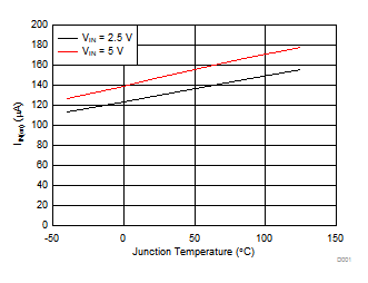
| RILIM = 36 KΩ | ||
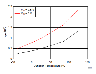
| RILIM = 36 KΩ | ||
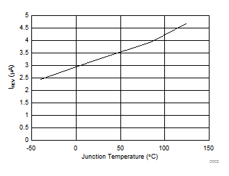
| VEN = VIN = 0 V | VOUT = 6.5 V | |
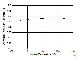
| CL = 1 µF | RL = 100 Ω | VIN = 6.5 V |
