-
TPS27082L 1.2-V to 8-V, 3-A PFET Load Switch With Configurable Slew Rate, Fast Transient Isolation and Hysteretic Control
- 1 Features
- 2 Applications
- 3 Description
- 4 Revision History
- 5 Pin Configuration and Functions
- 6 Specifications
- 7 Detailed Description
-
8 Application and Implementation
- 8.1 Application Information
- 8.2 Typical Application
- 8.3
System Examples
- 8.3.1 TFT LCD Module Inrush Current Control
- 8.3.2 Standby Power Isolation
- 8.3.3 Boost Regulator With True Shutdown
- 8.3.4 Single Module Multiple Power Supply Sequencing
- 8.3.5 Multiple Modules Interdependent Power Supply Sequencing
- 8.3.6 Multiple Modules Interdependent Supply Sequencing Without a GPIO Input
- 9 Power Supply Recommendations
- 10Layout
- 11Device and Documentation Support
- 12Mechanical, Packaging, and Orderable Information
- IMPORTANT NOTICE
Package Options
Mechanical Data (Package|Pins)
- DDC|6
Thermal pad, mechanical data (Package|Pins)
Orderable Information
TPS27082L 1.2-V to 8-V, 3-A PFET Load Switch With Configurable Slew Rate, Fast Transient Isolation and Hysteretic Control
1 Features
- Low ON-Resistance, High Current PFET
- RON = 32 mΩ (Typical) at VGS = –4.5 V
- RON = 44 mΩ (Typical) at VGS = –3.0 V
- RON = 85 mΩ (Typical) at VGS = –1.8 V
- RON = 97 mΩ (Typical) at VGS = –1.5 V
- RON = 155 mΩ (Typical) at VGS = –1.2 V
- Configurable Turn-ON and Turn-OFF Slew Rate
- 10-µs Default Minimum Output Rise Time at VIN=5 V
- Configurable Turnon and Turnoff Slew Rate
- Supports a Wide Range of VIN 1.2 V Up to 8 V
- Excellent OFF Isolation Even Under Fast Input Transients
- 1.0V up to 8V NMOS Control Logic Interface With Configurable Hystersis
- Fully Protected Against ESD (All Pins)
- HBM 2000 V, CDM 500 V
- Very Low ON-state Quiescent Current (Down to 1.2 µA)
- Very Low OFF-state Leakage Current (Typical 100 nA)
- Available in 2.9 mm × 1.6 mm x 0.75mm SOT-23 (DDC) Package
2 Applications
- High-Side Load Switches
- Inrush-current Controls
- Power Sequencing and Controls
- Stand-by Power Isolation
- Portable Power Switches
3 Description
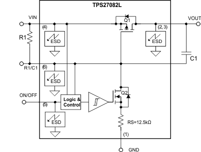
The TPS27082L IC is a high-side load switch that integrates a Power PFET and a control circuit in a tiny TSOT-23 package. TPS27082L requires very low ON-state quiescent current and offers very low OFF-state leakage thus optimizing system power efficiency.
TPS27082L ON/OFF logic interface features hysteresis, thus providing a robust logic interface even under very noisy operating conditions. TPS27082L ON/OFF interface supports direct interfacing to low voltage GPIOs down to 1 V. The TPS27082L level shifts ON/OFF logic signal to VIN levels without requiring an external level shifter.
TPS27082L features a novel OFF isolation circuit that prevents PMOS from turning ON in applications that may have fast transients, at the VIN pin when the load switch is in the OFF-state.
Device Information(1)
| PART NUMBER | PACKAGE | BODY SIZE (NOM) |
|---|---|---|
| TPS27082DDC | SOT (6) | 2.90 mm × 1.60 mm |
- For all available packages, see the orderable addendum at the end of the data sheet.
Simplified Schematic
