-
TPS27S100x 40-V, 4-A, 80-mΩ Single-Channel High-Side Switch
- 1 Features
- 2 Applications
- 3 Description
- 4 Revision History
- 5 Pin Configuration and Functions
- 6 Specifications
- 7 Detailed Description
- 8 Application and Implementation
- 9 Power Supply Recommendations
- 10Layout
- 11Device and Documentation Support
- 12Mechanical, Packaging, and Orderable Information
- IMPORTANT NOTICE
Package Options
Mechanical Data (Package|Pins)
Thermal pad, mechanical data (Package|Pins)
- PWP|14
Orderable Information
DATA SHEET
TPS27S100x 40-V, 4-A, 80-mΩ Single-Channel High-Side Switch
1 Features
- 80-mΩ Single-channel High-side switch with full diagnostics
- TPS27S100A: Open-drain status output
- TPS27S100B: Current monitor analog output
- Wide operating voltage 3.5 V to 40 V
- Very-low standby current, <0.5 µA
- Operating junction temperature, –40 to 150°C
- Input control, 3.3-V and 5-V logic compatible
- High-accuracy current monitor, ±30 mA at 1 A
- Adjustable current limit (0.5-A to 6-A) with external resistor, ±20% at 0.5 A
- Diagnostic enable function for multiplexing of MCU, analog or digital interface
- Excellent ESD protection on IN and OUT pins
- ±16 kV IEC 61000-4-2 ESD contact discharge
- ±4 kV IEC 61000-4-4 Electrical fast transient
- ±1.0 kV/42 Ω IEC 61000-4-5 Surge
- Protection
- Overload and short-circuit-to-GND protection
- Inductive load negative voltage clamp
- Undervoltage lockout (UVLO) protection
- Thermal shutdown and swing with self recovery
- Loss of GND protection
- Diagnostic
- On- and Off-State output Open-Load / short to supply detection
- Overload and short to ground detection
- Thermal shutdown and swing detection
- Thermally-Enhanced 14-Pin PWP or 16-Pin QFN package
2 Applications
- Programmable logic controller
- Building automation
- Telecom/networks
3 Description
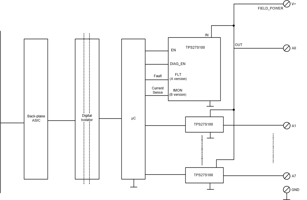
The TPS27S100x is a single-channel, fully-protected, high-side switch with an integrated NMOS and charge pump. Full diagnostics and high-accuracy current-monitor features enable intelligent control of the load. An adjustable current-limit function greatly improves the reliability of the whole system. The device diagnostic reporting has two versions to support both digital fault status and analog current monitor output. Accurate current monitor and adjustable current limit features differentiate it from the market.
Device Information(1)
| PART NUMBER | PACKAGE | BODY SIZE (NOM) |
|---|---|---|
| TPS27S100x | HTSSOP (14) | 4.40 mm × 5.00 mm |
| QFN (16) | 4.00 mm × 3.5 mm |
- For all available packages, see the orderable addendum at the end of the data sheet.
4 Revision History
Changes from A Revision (February 2018) to B Revision
- Added the QFN Package to the Features section Go
- Added Package QFN (16) and Body Size 4.00 mm × 3.5 mm to the Device Information tableGo
- Updated the Typical Application SchematicGo
- Added RRK Package to the Pin Out Drawing and Pin Functions tableGo
- Updated the SpecificationsAbsolute Maximum Ratings table Go
- Changed the Operation junction temperature range MAX from 150°C to 125°C in the SpecificationsRecommended Operating Conditions table Go
- Added RRK package to the Specifications Thermal Information tableGo
- Updated the Operating Current section in the SpecificationsElectrical Characteristics tableGo
Changes from * Revision (October 2017) to A Revision
- Added footnote 2 and 3 to the Electrical Characteristics tableGo
- Added reverse current protection information to the Reverse Current Protection sectionGo
5 Pin Configuration and Functions
TPS27S100B PWP Package
14-Pin HTSSOP With Exposed Thermal Pad
Top View
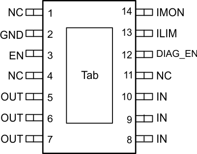
NC – No internal connection
TPS27S100A RRK Package
16-Pin QFN With Exposed Thermal Pad
Top View
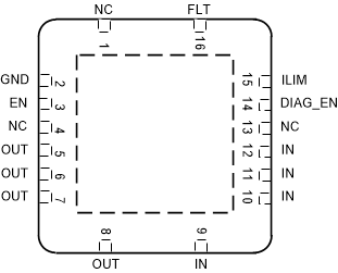
NC – No internal connection
TPS27S100B RRK Package
16-Pin QFN With Exposed Thermal Pad
Top View
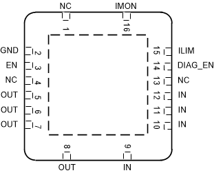
NC – No internal connection
Pin Functions
| PIN | I/O | DESCRIPTION | ||||
|---|---|---|---|---|---|---|
| NAME | TPS27S100A PWP | TPS27S100B PWP | TPS27S100A RRK | TPS27S100B RRK | ||
| DIAG_EN | 12 | 12 | 14 | 14 | I | Enable and disable pin for diagnostic functions. Connect to device GND if not used. |
| EN | 3 | 3 | 3 | 3 | I | Enable control for channel activation. |
| FLT | 14 | — | 16 | — | O | Open-drain diagnostic status output. Leave floating if not used. |
| GND | 2 | 2 | 2 | 2 | — | Ground pin. |
| ILIM | 13 | 13 | 15 | 15 | O | adjustable current-limit pin. Connect to device GND if external current limit is not used. |
| IMON | — | 14 | — | 16 | O | Current-monitor output. Leave floating if not used. |
| IN | 8, 9, 10 | 8, 9, 10 | 9, 10, 11, 12 | 9, 10, 11, 12 | I | Power supply. |
| NC | 1, 4, 11 | 1, 4, 11 | 1, 4, 13 | 1, 4, 13 | — | No-connect pin; leave floating. |
| OUT | 5, 6, 7 | 5, 6, 7 | 5, 6, 7, 8 | 5, 6, 7, 8 | O | Output, connected to load. |
| Thermal pad | — | — | — | — | — | Thermal pad. Connect to device GND or leave floating. |
6.1 Absolute Maximum Ratings
over operating ambient temperature range (unless otherwise noted) (1)(2)| MIN | MAX | UNIT | |
|---|---|---|---|
| Supply voltage | 40 | V | |
| Supply voltage (for transients less than 400 ms) | 48 | V | |
| Current on GND pin, t < 2 minutes | –250 | 100 | mA |
| Voltage on EN and DIAG_EN pins | –0.3 | 7 | V |
| Current on EN and DIAG_EN pins | –10 | mA | |
| Voltage on FLT pin | –0.3 | 7 | V |
| Current on FLT pin | –30 | 10 | mA |
| Voltage on ILIM pin | –0.3 | 7 | V |
| Voltage on IMON pin | –2.7 | 6.5 | V |
| Inductive load switch-off energy dissipation, single pulse(3) | 70 | mJ | |
| Operating junction temperature, TJ | –40 | 150 | °C |
| Storage temperature, Tstg | –65 | 150 | °C |
(1) Stresses beyond those listed under Absolute Maximum Ratings may cause permanent damage to the device. These are stress ratings only, which do not imply functional operation of the device at these or any other conditions beyond those indicated under Recommended Operating Conditions. Exposure to absolute-maximum-rated conditions for extended periods may affect device reliability.
(2) All voltage values are with respect to GND.
(3) Test condition: VIN = 13.5 V, L = 8 mH, R = 0 Ω, TJ = 150°C. FR4 2s2p board, 2- × 70-μm Cu, 2- × 35-μm Cu. 600-mm2 board copper area.
6.2 ESD Ratings
| VALUE | UNIT | ||||
|---|---|---|---|---|---|
| V(ESD) | Electrostatic discharge | Human body model (HBM) (1) | IN, OUT, GND | ±5000 | V |
| Human body model (HBM) (1) | Other pins | ±4000 | |||
| Charged device model (CDM) | ±750 | ||||
| V(ESD) | Electrostatic discharge | Contact/Air discharge, per IEC 61000-4-2 (2) | IN, OUT | ±16000 | V |
| V(ESD) | Electrical fast transient, per IEC 61000-4-4 (2) | IN, OUT | ±4000 | V | |
| V(ESD) | Surge protection with 42 Ω, per IEC 61000-4-5; 1.2/50 μs (2) | IN, OUT | ±1000 | V | |
(1) JEDEC document JEP155 states that 500-V HBM allows safe manufacturing with a standard ESD control process.
(2) Tested with application circuit shown in Figure 35 with CVIN1= 47 μF, CVIN2= 100 nF, CVOUT= 22 nF and SM15T30A TVS input clamp. Supply voltage of 24 V DC is always ON, EN Inputs are High, so output is High (ON) and floating (no load).
6.3 Recommended Operating Conditions
over operating free-air temperature range (unless otherwise noted)| MIN | MAX | UNIT | ||
|---|---|---|---|---|
| VIN | Operating voltage | 5 | 40 | V |
| VENx | Voltage on EN and DIAG_EN pins | 0 | 5 | V |
| VFLT | Voltage on FLT pin | 0 | 5 | V |
| IL,nom | Nominal dc load current | 0 | 4 | A |
| TJ | Operating junction temperature range | –40 | 125 | °C |
