SLUSCJ3A April 2016 – June 2016 TPS53632G
PRODUCTION DATA.
- 1 Features
- 2 Applications
- 3 Description
- 4 Revision History
- 5 Pin Configuration and Functions
- 6 Specifications
- 7 Timing Requirements
- 8 Switching Characteristics
- 9 Typical Characteristics (Half-Bridge Operation)
-
10Detailed Description
- 10.1 Overview
- 10.2 Functional Block Diagram
- 10.3
Feature Description
- 10.3.1 Current Sensing
- 10.3.2 Load Transients
- 10.3.3 PWM and SKIP Signals
- 10.3.4 5-V, 3.3-V and 1.8-V Undervoltage Lockout (UVLO)
- 10.3.5 Output Undervoltage Protection (UVP)
- 10.3.6 Overcurrent Protection (OCP)
- 10.3.7 Overvoltage Protection
- 10.3.8 Analog Current Monitor, IMON and Corresponding Digital Output Current
- 10.3.9 Addressing
- 10.3.10 I2C Interface Operation
- 10.3.11 Start-Up Sequence
- 10.3.12 Power Good Operation
- 10.3.13 Fault Behavior
- 10.4 Device Functional Modes
- 10.5 Configuration and Programming
- 10.6 Register Maps
-
11Applications and Implementation
- 11.1 Application Information
- 11.2
Typical Application
- 11.2.1
D-CAP+™ Half-Bridge Application
- 11.2.1.1 Design Requirements
- 11.2.1.2
Detailed Design Procedure
- 11.2.1.2.1 Step 1: Select Switching Frequency
- 11.2.1.2.2 Step 2: Set The Slew Rate
- 11.2.1.2.3 Step 3: Determine Inductor Value And Choose Inductor
- 11.2.1.2.4 Step 4: Determine Current Sensing Method
- 11.2.1.2.5 Step 5: DCR Current Sensing
- 11.2.1.2.6 Step 6: Select OCP Level
- 11.2.1.2.7 Step 7: Set the Load-Line Slope
- 11.2.1.2.8 Step 8: Current Monitor (IMON) Setting
- 11.2.1.3 Application Performance Plots
- 11.2.1.4 Loop Compensation for Zero Load-Line
- 11.2.1
D-CAP+™ Half-Bridge Application
- 12Power Supply Recommendations
- 13 Layout
- 14Device and Documentation Support
- 15Mechanical, Packaging, and Orderable Information
Package Options
Mechanical Data (Package|Pins)
- RSM|32
Thermal pad, mechanical data (Package|Pins)
- RSM|32
Orderable Information
1 Features
- Valley Current Mode with Constant ON Time Control
- Lossless Current Sensing Scheme
- I2C Interface for VID Control and Telemetry
- Programmable I2C Addresses up to Eight Devices
- Switching Frequency up to 1 MHz
- Digital Current Monitor
- 7-Bit, DAC Output Range: 0.50-V to 1.52-V with 10-mV Step
- Accurate, Adjustable Voltage Positioning or Zero Slope Load-Line
- Selectable, 8-Level Current Limit
- Adjustable Output Slew Rate Control
- Default Boot Voltage: 1.00 V
- Small, 4-mm × 4-mm, 32-Pin, VQFN, PowerPAD Package
2 Applications
- 48-V Point-of-Load (POL) for Data Center and Telecommunication
- Wide Input Range Power Supplies for Industrial
3 Description
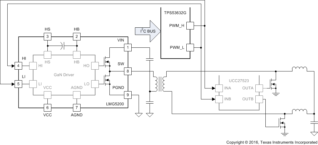
The TPS53632G device is a half-bridge PWM controller with D-CAP+™ architecture that provides fast transient response, lowest output capacitance and high efficiency in single stage conversion directly from 48-V bus. The TPS53632G device supports the standard I2C Rev 3.0 interface for dynamic control of the output voltage and current monitor telemetry. Paired with TI GaN power stages and drivers, the TPS53632G can switch up to 1 MHz to minimize magnetic component size and reduce overall board space. The LMG5200 GaN power stage is designed specifically for this controller to achieve high frequency and efficiency as high as 92% with 48-V to 1-V conversion.
Other features include adjustable control of output slew rate and voltage positioning. In addition, the TPS53632G device can be used along with other TI discrete power MOSFETs and drivers for silicon-based half bridge solutions. The TPS53632G device is packaged in a space saving, thermally enhanced, 32-pin VQFN package and is rated to operate at a range between –10°C and 105°C.
Device Information
| PART NUMBER | PACKAGE | BODY SIZE |
|---|---|---|
| TPS53632G | VQFN | 4 mm × 4 mm |
WHITESPACE
WHITESPACE
Simplified Schematic
