SLVSC61A November 2013 – October 2016 TPS54341
PRODUCTION DATA.
- 1 Features
- 2 Applications
- 3 Description
- 4 Revision History
- 5 Pin Configuration and Functions
- 6 Specifications
-
7 Detailed Description
- 7.1 Overview
- 7.2 Functional Block Diagram
- 7.3
Feature Description
- 7.3.1 Fixed Frequency PWM Control
- 7.3.2 Slope Compensation Output Current
- 7.3.3 Low Dropout Operation and Bootstrap Voltage (BOOT)
- 7.3.4 Error Amplifier
- 7.3.5 Adjusting the Output Voltage
- 7.3.6 Enable and Adjusting Undervoltage Lockout
- 7.3.7 Soft-Start/Tracking Pin (SS/TR)
- 7.3.8 Sequencing
- 7.3.9 Constant Switching Frequency and Timing Resistor (RT/CLK Pin)
- 7.3.10 Accurate Current Limit Operation and Maximum Switching Frequency
- 7.3.11 Synchronization to RT/CLK Pin
- 7.3.12 Power Good (PWRGD Pin)
- 7.3.13 Overvoltage Protection
- 7.3.14 Thermal Shutdown
- 7.3.15 Small-Signal Model for Loop Response
- 7.3.16 Simple Small-Signal Model for Peak-Current-Mode Control
- 7.3.17 Small Signal Model for Frequency Compensation
- 7.4 Device Functional Modes
-
8 Application and Implementation
- 8.1 Application Information
- 8.2
Typical Application
- 8.2.1 Design Requirements
- 8.2.2
Detailed Design Procedure
- 8.2.2.1 Selecting the Switching Frequency
- 8.2.2.2 Output Inductor Selection (LO)
- 8.2.2.3 Output Capacitor
- 8.2.2.4 Catch Diode
- 8.2.2.5 Input Capacitor
- 8.2.2.6 Slow-Start Capacitor
- 8.2.2.7 Bootstrap Capacitor Selection
- 8.2.2.8 Undervoltage Lockout Set Point
- 8.2.2.9 Output Voltage and Feedback Resistors Selection
- 8.2.2.10 Compensation
- 8.2.2.11 Discontinuous Conduction Mode and Eco-mode Boundary
- 8.2.2.12 Estimated Circuit Area
- 8.2.2.13 Power Dissipation Estimate
- 8.2.3 Application Curves
- 9 Power Supply Recommendations
- 10Layout
- 11Device and Documentation Support
- 12Mechanical, Packaging, and Orderable Information
Package Options
Mechanical Data (Package|Pins)
- DPR|10
Thermal pad, mechanical data (Package|Pins)
- DPR|10
Orderable Information
1 Features
- High Efficiency at Light Loads with Pulse Skipping Eco-mode™
- 87-mΩ High-Side MOSFET
- 152-μA Operating Quiescent Current and
2-μA Shutdown Current - 100-kHz to 2.5-MHz Adjustable Switching Frequency
- Synchronizes to External Clock
- Low Dropout at Light Loads with Integrated BOOT Recharge FET
- Adjustable UVLO Voltage and Hysteresis
- UV and OV Power-Good Output
- Adjustable Soft-Start and Sequencing
- 0.8-V 1% Internal Voltage Reference
- 10-Pin WSON with Thermal Pad Package
- –40°C to 150°C TJ Operating Range
- Supported by WEBENCH® Software Tool
2 Applications
- Industrial Automation and Motor Control
- Vehicle Accessories: GPS and Entertainment (see Creating GSM/GRPS Power Supply from TPS54260, SLVA412)
- USB-Dedicated Charging Ports and Battery Chargers (see Creating a Universal Car Charger for USB devices From the TPS54240 and TPS2511, SLVA464)
- 12-V and 24-V Industrial, Automotive and Communications Power Systems
3 Description
The TPS54341 device is a 42-V, 3.5-A step-down regulator with an integrated high-side MOSFET. The device survives load-dump pulses up to 45 V per ISO 7637. Current mode control provides simple external compensation and flexible component selection. A low-ripple pulse-skip mode reduces the no-load supply current to 152 μA. Shutdown supply current is reduced to 2 μA when the enable pin is pulled low.
Undervoltage lockout is internally set at 4.3 V but can increase using an external resistor divider at the enable pin. The output voltage startup ramp is controlled by the soft start pin that can also be configured for sequencing/tracking. An open-drain power-good signal indicates the output is within 93% to 106% of the nominal voltage.
A wide adjustable switching-frequency range allows for optimization of either efficiency or external component size. Cycle-by-cycle current limit, frequency foldback and thermal shutdown protects internal and external components during an overload condition.
The TPS54341 device is available in a 10-pin 4-mm × 4-mm WSON package.
Device Information(1)
| PART NUMBER | PACKAGE | BODY SIZE (NOM) |
|---|---|---|
| TPS54341 | WSON (10) | 4.00 mm × 4.00 mm |
- For all available packages, see the orderable addendum at the end of the data sheet.
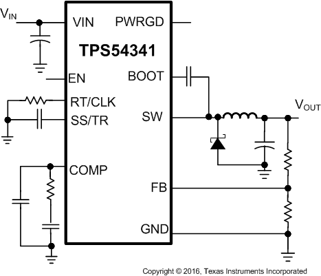
Simplified Schematic

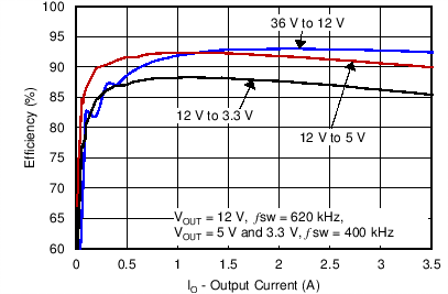
Efficiency vs Load Current
