-
TPS54821 4.5 V to 17 V Input, 8 A Synchronous Step Down Converter With Hiccup
- 1 Features
- 2 Applications
- 3 Description
- 4 Revision History
- 5 Pin Configuration and Functions
- 6 Specifications
-
7 Detailed Description
- 7.1 Overview
- 7.2 Functional Block Diagram
- 7.3 Feature Description
- 7.4
Device Functional Modes
- 7.4.1 Enable and Adjusting Undervoltage Lockout
- 7.4.2 Adjustable Switching Frequency and Synchronization (RT/CLK)
- 7.4.3 Adjustable Switching Frequency (RT Mode)
- 7.4.4 Synchronization (CLK mode)
- 7.4.5 Slow Start (SS/TR)
- 7.4.6 Power Good (PWRGD)
- 7.4.7 Bootstrap Voltage (BOOT) and Low Dropout Operation
- 7.4.8 Sequencing (SS/TR)
- 7.4.9 Output Overvoltage Protection (OVP)
- 7.4.10 Overcurrent Protection
- 7.4.11 Thermal Shutdown
- 7.4.12 Small Signal Model for Loop Response
- 7.4.13 Simple Small Signal Model for Peak Current Mode Control
- 7.4.14 Small Signal Model for Frequency Compensation
-
8 Application and Implementation
- 8.1 Application Information
- 8.2
Typical Application
- 8.2.1 Design Parameters
- 8.2.2
Design Guide - Step-By-Step Design Procedure
- 8.2.2.1 Typical Application Schematic
- 8.2.2.2 Operating Frequency
- 8.2.2.3 Output Inductor Selection
- 8.2.2.4 Output Capacitor Selection
- 8.2.2.5 Input Capacitor Selection
- 8.2.2.6 Slow Start Capacitor Selection
- 8.2.2.7 Bootstrap Capacitor Selection
- 8.2.2.8 Under Voltage Lockout Set Point
- 8.2.2.9 Output Voltage Feedback Resistor Selection
- 8.2.2.10 Compensation Component Selection
- 8.2.2.11 Fast Transient Considerations
- 8.2.3 Application Curves
- 9 Power Supply Recommendations
- 10Layout
- 11Device and Documentation Support
- 12Mechanical, Packaging, and Orderable Information
- IMPORTANT NOTICE
Package Options
Mechanical Data (Package|Pins)
- RHL|14
Thermal pad, mechanical data (Package|Pins)
Orderable Information
TPS54821 4.5 V to 17 V Input, 8 A Synchronous Step Down Converter With Hiccup
1 Features
- Integrated 26 mΩ / 19 mΩ MOSFETs
- Split Power Rail: 1.6 V to 17 V on PVIN
- 200 kHz to 1.6 MHz Switching Frequency
- Synchronizes to External Clock
- 0.6V ±1% Voltage Reference Over Temperature
- Low 2 µA Shutdown Quiescent Current
- Monotonic Start-Up into Pre-biased Outputs
- Adjustable Slow Start/Power Sequencing
- Power Good Output Monitor for Undervoltage and Overvoltage
- Adjustable Input Undervoltage Lockout
- Software Tools Available
2 Applications
- Digital TV Power Supplies
- Set Top Boxes
- Blu-ray DVDs
- Home Terminals
- High Performance Point of Load Regulation
3 Description
The TPS54821 in thermally enhanced 3.5 mm x 3.5 mm QFN package is a full featured 17 V, 8 A synchronous step down converter which is optimized for small designs through high efficiency and integrating the high-side and low-side MOSFETs. Further space savings are achieved through current mode control, which reduces component count, and by selecting a high switching frequency, reducing the inductor's footprint.
The output voltage startup ramp is controlled by the SS/TR pin which allows operation as either a stand alone power supply or in tracking situations. Power sequencing is also possible by correctly configuring the enable and the open drain power good pins.
Cycle by cycle current limiting on the high-side FET protects the device in overload situations and is enhanced by a low-side sourcing current limit which prevents current runaway. There is also a low-side sinking current limit which turns off the low-side MOSFET to prevent excessive reverse current. Hiccup protection will be triggered if the overcurrent condition has persisted for longer than the preset time. Thermal hiccup protection disables the device when the die temperature exceeds the thermal shutdown temperature and enables the part again after the built-in thermal shutdown hiccup time.
Device Information(1)
| PART NUMBER | PACKAGE | BODY SIZE (NOM) |
|---|---|---|
| TPS54821 | VQFN (14) | 3.50 mm x 3.50 mm |
- For all available packages, see the orderable addendum at the end of the datasheet.
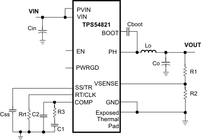
Simplified Schematic

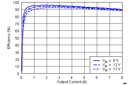
Efficiency, VOUT = 3.3 V, FSW = 480 kHz

4 Revision History
Changes from A Revision (November 2014) to B Revision
- Deleted SWIFT™ from the data sheet title Go
- Deleted Features: For SWIFT™ Documentation visit http://www.ti.com/swiftGo
- Moved Storage temperature to the Absolute Maximum RatingsGo
- Changed Handling Ratings to ESD Ratings Go
Changes from * Revision (October 2011) to A Revision
- Added Handling Rating table, Feature Description section, Device Functional Modes, Application and Implementation section, Power Supply Recommendations section, Layout section, Device and Documentation Go
- Deleted Feature: –40°C to 125°C Operating Junction Temperature Range Go
- Added the I/O column to the Pin Functions table Go
- Added IOUT = 8A and IOUT = 6A to the Operating Junction Temperature row of the ABS MAX table, also Min = -40 and Max =150 Go
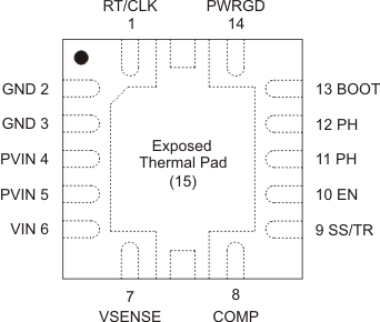
5 Pin Configuration and Functions
