-
TPS65133 ±5-V, 250-mA Dual-Output Power Supply
- 1 Features
- 2 Applications
- 3 Description
- 4 Typical Application
- 5 Revision History
- 6 Pin Configuration and Functions
- 7 Specifications
- 8 Detailed Description
- 9 Application and Implementation
- 10Power Supply Recommendations
- 11Layout
- 12Device and Documentation Support
- 13Mechanical, Packaging, and Orderable Information
- IMPORTANT NOTICE
Package Options
Mechanical Data (Package|Pins)
- DPD|12
Thermal pad, mechanical data (Package|Pins)
- DPD|12
Orderable Information
TPS65133 ±5-V, 250-mA Dual-Output Power Supply
1 Features
- 2.9-V to 5.0-V Input Voltage Range
- Fixed 5.0-V Positive Output Voltage (VPOS)
- Fixed –5.0-V Negative Output Voltage (VNEG)
- ±1% Output Voltage Accuracy
- High Efficiency
- 250-mA Output Current Capability
- Independent Converter Operation Allows 100% Output Current Mismatch
- Excellent Line and Load Transient Response
- Operates in CCM to Minimize Output Noise
- Boost Converter able to Operate with Input Supply Voltages close to 5.0 V
- Short-Circuit Protection
- Thermal Shutdown
2 Applications
- LCD Bias
- AMOLED Supplies
- Operational Amplifier Supplies
- Headphone Amplifier Supplies
- Sensor Front-End Supplies
- Data Acquisition Supplies
- General ±5-V Power Supplies
3 Description
The TPS65133 is designed to supply any system requiring ±5.0-V supply rails. Each output can supply up to 250 mA of output current. The input supply voltage range is suitable for use with lithium ion batteries or from a fixed 3.3-V supply.
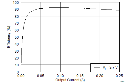
Efficiency is typically over 90% for most applications (operating from a lithium ion battery, output currents in the range 50 mA to 200 mA). The two converters in the TPS65133 device operate independently, allowing 100% mismatch between positive and negative output currents.
Device Information(1)
| PART NUMBER | PACKAGE | BODY SIZE (NOM) |
|---|---|---|
| TPS65133 | WSON (12) | 3.00 mm × 3.00 mm |
- For all available packages, see the orderable addendum at the end of the datasheet.
5 Revision History
Changes from * Revision (June 2013) to A Revision
- Added Device Information table, ESD Ratings table, Switching Characteristics table, Feature Description section, Device Functional Modes, Application and Implementation section, Power Supply Recommendations section, Device and Documentation Support section, and Mechanical, Packaging, and Orderable Information section. Go
- Changed Layout Example Go
6 Pin Configuration and Functions
Pin Functions
| PIN | DESCRIPTION | |
|---|---|---|
| NAME | NO. | |
| AGND | 5 | Analog ground |
| AVIN | 11 | Internal logic supply pin |
| EN | 7 | Enable of boost and buck-boost converter |
| GND | 4, 6, 8 | Ground |
| SWP | 1 | Switch pin of the boost converter |
| PGND | 2 | Power ground of the boost converter |
| PVIN | 12 | Supply pin for the negative buck-boost converter. Place a capacitor close to this pin. |
| SWN | 10 | Switch pin of the negative buck-boost converter |
| VNEG | 9 | Output of the negative buck-boost converter (VNEG), place a capacitor close to this pin. |
| VPOS | 3 | Output of the boost converter (VPOS), place a capacitor close to this pin. |
| Exposed thermal pad | Exposed thermal pad. Connect this pad to all GND pins. | |
7 Specifications
7.1 Absolute Maximum Ratings(1)
over operating free-air temperature range (unless otherwise noted)| MIN | MAX | UNIT | ||
|---|---|---|---|---|
| Input voltage(2) | PVIN, AVIN, EN, SWP, VPOS | –0.3 | 6 | V |
| VNEG | –6.5 | 0.3 | V | |
| SWN | –6.5 | 5.5 | V | |
| Junction temperature, TJ | –40 | 150 | °C | |
| Storage temperature, Tstg | –65 | 150 | °C | |
7.2 ESD Ratings
| VALUE | UNIT | |||
|---|---|---|---|---|
| V(ESD) | Electrostatic discharge | Human-body model (HBM), per ANSI/ESDA/JEDEC JS-001(1) | ±2000 | V |
| Charged-device model (CDM), per JEDEC specification JESD22-C101(2) | ±500 | |||
7.3 Recommended Operating Conditions(1)
over operating free-air temperature range (unless otherwise noted)| MIN | NOM | MAX | UNIT | ||
|---|---|---|---|---|---|
| VI | Input voltage | 2.9 | 3.7 | 5 | V |
| TA | Operating ambient temperature | –40 | 85 | °C | |
| TJ | Operating junction temperature | –40 | 125 | °C | |
7.4 Thermal Information
| THERMAL METRIC(1) | TPS65133 | UNIT | |
|---|---|---|---|
| DPD (WSON) | |||
| 12 PINS | |||
| RθJA | Junction-to-ambient thermal resistance | 51.5 | °C/W |
| RθJC(top) | Junction-to-case (top) thermal resistance | 41.7 | |
| RθJB | Junction-to-board thermal resistance | 25 | |
| ψJT | Junction-to-top characterization parameter | 0.5 | |
| ψJB | Junction-to-board characterization parameter | 25.2 | |
| RθJC(bot) | Junction-to-case (bottom) thermal resistance | 4.4 | |
7.5 Electrical Characteristics
VI = 3.7 V, EN = VI, VPOS = 5.0 V, VNEG = –5.0 V, TA = –40°C to 85°C, typical values are at TA = 25°C (unless otherwise noted)7.6 Switching Characteristics
over operating free-air temperature range (unless otherwise noted)| PARAMETER | TEST CONDITIONS | MIN | TYP | MAX | UNIT | |
|---|---|---|---|---|---|---|
| BOOST CONVERTER (VPOS) | ||||||
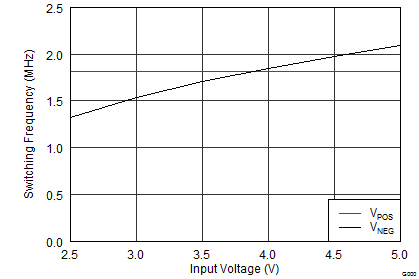
| Switching frequency | IPOS = 200 mA | 1.2 | 1.7 | 2.2 | MHz | |
| Short-circuit detection time | The delay from when VPOS < V(SCP)(P) to when the boost converter turns off | 1 | 3 | 5 | ms | |
| BUCK-BOOST CONVERTER (VNEG) | ||||||
| Switching frequency | INEG = –200 mA | 1 | 1.7 | 2.4 | MHz | |
| Short-circuit detection time | The delay from when VNEG > V(SCP)(N) to when the inverting buck-boost converter turns off | 1 | 3 | 5 | ms | |
| Start-up delay | The delay from when VPOS has reached its target value to when VNEG starts ramping | 2 | ms | |||
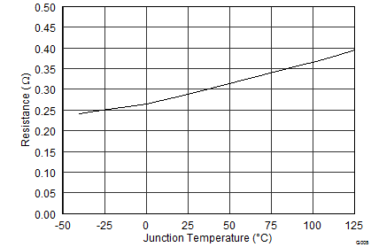
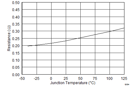
7.7 Typical Characteristics
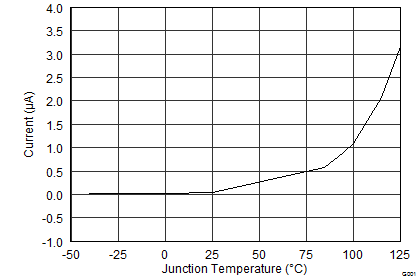
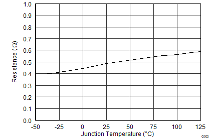

8 Detailed Description
8.1 Overview
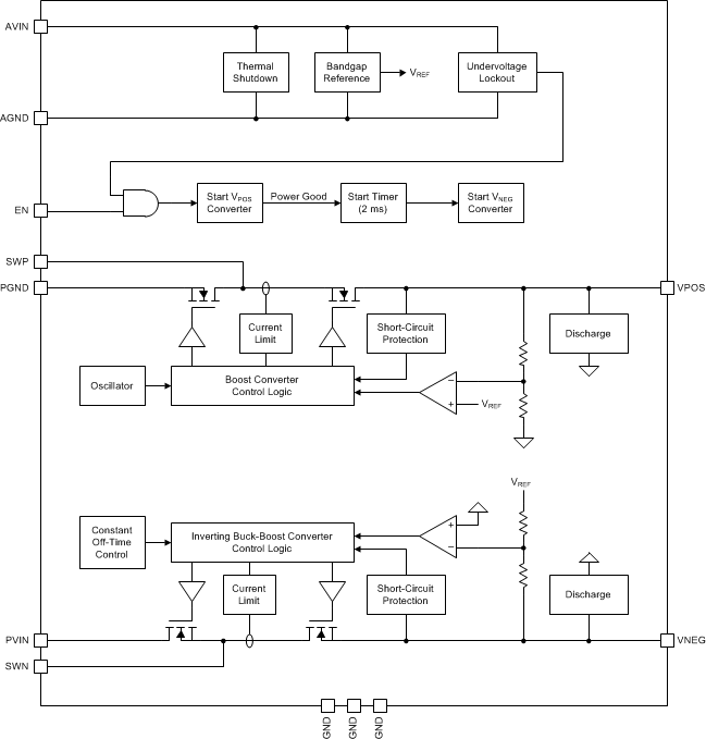
The TPS65133 device comprises a boost converter and an inverting buck-boost converter. The boost converter generates a positive output voltage of 5.0 V and the inverting buck-boost converter generates a negative output voltage of –5.0 V. Both converters have an output voltage accuracy of ±1%.
8.2 Functional Block Diagram
8.3 Feature Description
8.3.1 Boost Converter (VPOS)
The boost converter uses a current-mode topology with synchronous rectification (see Figure 6). The synchronous rectifier improves efficiency and provides input-output isolation when the converter is disabled. When the input supply voltage is close 5.0 V, preventing normal boost operation, the synchronous rectifier is disabled, allowing the output voltage regulation to be maintained (see Operation with VI ≈ VPOS (Diode Mode)).
 Figure 6. VPOS Boost Converter Internal Block Diagram
8.3.1.1 Switching Frequency (VPOS)
The boost converter switching frequency may vary slightly as the operating conditions change, but is typically around 1.7 MHz for most operating conditions.
8.3.1.2 Output Voltage (VPOS)
The boost converter's output voltage is factory-programmed to 5.0 V ±1.0% and cannot be changed by the user.
8.3.1.3 Startup (VPOS)
The boost converter starts up as soon as EN=HIGH and the input supply voltage is above the UVLO threshold. The converter features an integrated soft-start function to control the ramp of its output voltage.
8.3.1.4 Shutdown (VPOS)
The boost converter shuts down when EN=LOW or the input supply voltage falls below the UVLO threshold.
8.3.1.5 Active Discharge (VPOS)
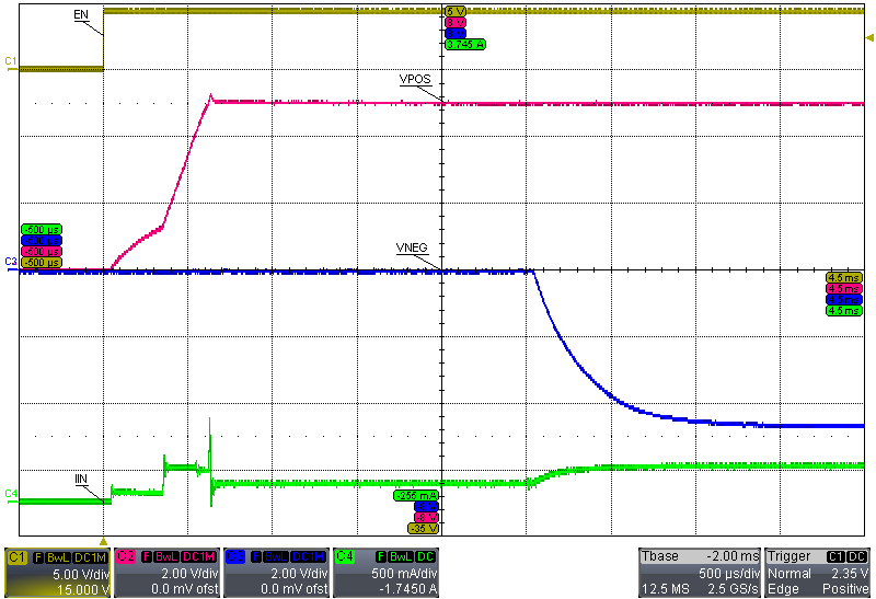
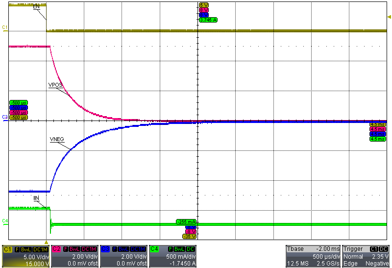
The boost converter output is actively discharged to ground when the converter is disabled (see Figure 8). During startup, active discharge begins as soon as the input supply voltage is above the UVLO threshold. During shutdown, active discharge persists until the input supply voltage is too low to support its operation (VI ≈ 1.5 V).
8.3.1.6 Short-Circuit Protection (VPOS)
The boost converter is protected against short-circuits on its output. If a short-circuit condition is detected during start-up, the converter limits its output current until the short-circuit condition is removed. Note that if a boost converter short-circuit condition is detected during start-up, the inverting buck-boost converter will not start until the condition is removed (because the sequencing logic requires VPOS to be in regulation before the inverting buck-boost converter is started).
During normal operation the boost converter detects a short-circuit on its output if VPOS < 4.1 V for longer than 3 ms. When a short-circuit condition is detected both VPOS and VNEG are disabled and the device shuts down. Normal operation is resumed by pulling EN low and then high again, or by cycling the input supply voltage.
8.3.2 Inverting Buck-Boost Converter (VNEG)
The inverting buck-boost converter uses a current-mode topology with synchronous rectification (see Figure 7).
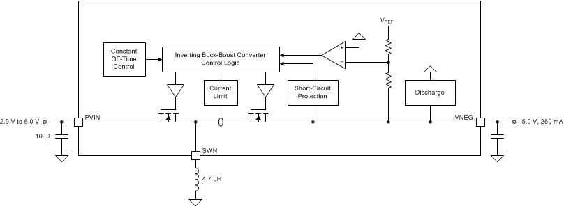 Figure 7. VNEG Buck-Boost Converter Internal Block Diagram
8.3.2.1 Switching Frequency (VNEG)
The inverting buck-boost converter's switching frequency varies slightly with operating conditions, but is approximately 1.7 MHz for most operating conditions.
8.3.2.2 Output Voltage (VNEG)
The inverting buck-boost converter's output voltage is factory-programmed to –5.0 V ±1.0% and cannot be changed by the user.
8.3.2.3 Startup (VNEG)
The inverting buck-boost converter starts up approximately 2 ms after the boost converter output has reached 5.0 V. The converter's switch current is limited during startup and the output voltage ramps in a controlled manner.
8.3.2.4 Shutdown
The inverting buck-boost converter shuts down when EN=LOW or the input supply voltage falls below the UVLO threshold.
8.3.2.5 Active Discharge (VNEG)
The inverting buck-boost converter output is actively discharged to ground when the converter is disabled (see Figure 8). During startup, active discharge begins as soon as the input supply voltage is above the UVLO threshold. During shutdown, active discharge persists until the input supply voltage is too low to support its operation (VI ≈ 1.5 V).
8.3.2.6 Short-Circuit Protection (VNEG)
The inverting buck-boost converter is protected against short-circuits on its output. If a short-circuit condition is detected during startup, the device converter limits its output current until the short-circuit condition is removed.
During normal operation the inverting buck-boost converter detects a short-circuit on its output if VNEG > –4.5 V for longer than 3 ms. When a short-circuit condition is detected both VPOS and VNEG are disabled and the device shuts down. Normal operation is resumed by pulling EN low and then high again, or by cycling the input supply voltage.
8.3.3 Startup and Shutdown Sequencing
Figure 8 illustrates the startup and shutdown sequencing of the TPS65133 device.
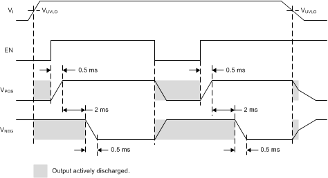 Figure 8. Startup and Shutdown Sequencing
8.3.4 Thermal Shutdown
The TPS65133 device features a thermal shutdown function to prevent damage because of excessive temperature. Once a junction temperature of 135°C (typical) is exceeded the device goes into shuts down. Normal operation is resumed (assuming that the device junction temperature has fallen below the thermal shut-down threshold) by pulling EN low and then high again, or by cycling the input supply voltage.
8.4 Device Functional Modes
8.4.1 Operation with VI < 2.9 V
The recommended minimum input supply voltage is 2.9 V. The device continues to operate with input supply voltages below 2.9 V, however, full performance is not guaranteed. The device does not operate with input supply voltages below the UVLO threshold.
8.4.2 Operation with VI ≈ VPOS (Diode Mode)
The TPS65133 device features a "diode" mode that enables it to regulate its positive output even when the input supply voltage is close to 5.0 V (i.e. too high for normal boost operation). When operating in diode mode the converter's synchronous rectifier stops switching and instead its body diode is used to rectify the output current. Boost converter efficiency is reduced in diode mode. At low output currents (≈2 mA and below), the boost converter automatically transitions from pulse-width modulation to pulse-skip operation. This ensures that the boost converter's output stays in regulation, but increases the voltage ripple on VPOS.
8.4.3 Operation with EN
When EN=LOW the TPS65133 device is disabled and switching is inhibited. When the input supply voltage is above the undervoltage lockout threshold and EN=HIGH the device is enabled and its start-up sequence begins.
9 Application and Implementation
NOTE
Information in the following applications sections is not part of the TI component specification, and TI does not warrant its accuracy or completeness. TI’s customers are responsible for determining suitability of components for their purposes. Customers should validate and test their design implementation to confirm system functionality.
9.1 Application Information
The TPS65133 device can be used to generate ±5-V supply rails from input supply voltages in the range 2.9 V to 5 V, and has been optimized for use with regulated 3.3-V rails and single-cell Li-Ion batteries. Its output voltages are fixed at ±5 V and cannot be changed by the user. Both output voltages are controlled by the EN pin: a high logic level on the EN pin enables both outputs, and a low logic level disables them. Note that when the input supply voltage is above the UVLO threshold and the EN pin is low, both outputs are disabled and actively discharged to ground. When the input supply voltage is below the UVLO threshold, both outputs are disabled, but they are not actively discharged.
9.2 Typical Application
Figure 9 shows a typical application schematic suitable for supplying up to 250 mA at ±5 V from e.g. a single-cell Li-Ion battery.
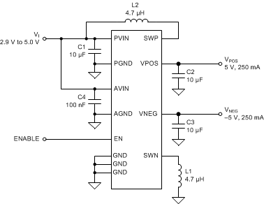 Figure 9. Typical Application Circuit
9.2.1 Design Requirements
The design parameters for the application circuit in Figure 9 are listed in Table 1.
Table 1. Design Parameters
| PARAMETERS | EXAMPLE VALUES |
|---|---|
| Input voltage range | 2.9 V to 5.0 V |
| Output voltage | ±5.0 V |
| Switching frequency | 1.7 MHz |
9.2.2 Detailed Design Procedure
In order to maximize performance, the TPS65133 device has been optimized for use with a relatively narrow range of external components, and customers are recommended to use the application circuit shown in Figure 9 and the components listed in Table 2 and Table 3.
9.2.2.1 Inductor Selection
The two dc-dc converters in the TPS65133 device have been optimized for use with 4.7 µH inductors, and it is recommended to use this value in all applications. Customers using different values of inductors should characterize performance thoroughly before going to mass production.
Table 2. Inductor Selection
| PARAMETER | VALUE | MANUFACTURER | PART NUMBER |
|---|---|---|---|
| L1, L2 | 4.7 µH | Coilmaster | MMPP252012-4R7N |
| Toko | 1239AS-H-4R7M | ||
| ABCO | LPP252012-4R7N | ||
| Coilcraft | XFL4020-4R7ML |
9.2.2.2 Capacitor Selection
The recommended capacitor values are shown in Table 3. Applications using less than the recommended capacitance (e.g. to save PCB area) may experience increased voltage ripple. In general, the lower the output power required by the application, the lower the capacitance needed for proper performance. C4 improves immunity to noise on the input supply voltage, but it is not necessary in many applications.
Table 3. Capacitor Selection
| PARAMETER | VALUE | MANUFACTURER | PART NUMBER |
|---|---|---|---|
| C1, C2, C3 | 10 µF | Murata | GRM21BR71A106KE51 |
| C4 | 100 nF | GRM21BR71E104KA01 |
9.2.3 Application Performance Graphs
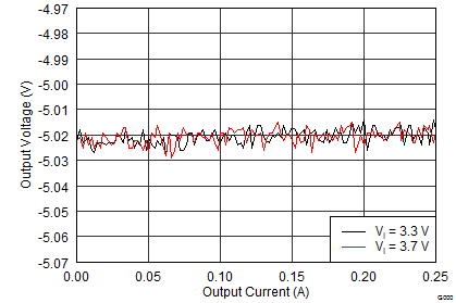
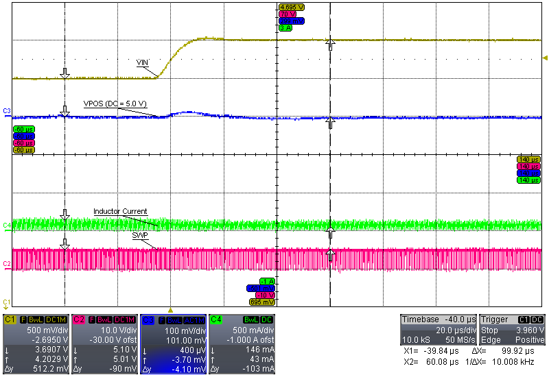
The performance shown in the following graphs was obtained using the circuit shown in Figure 9 and the external components listed in Table 2 and Table 3.
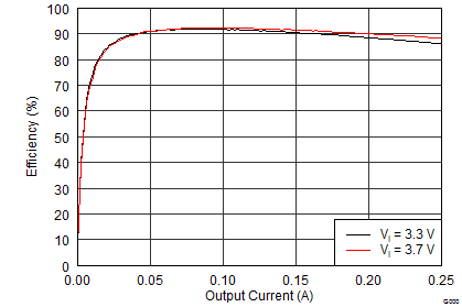
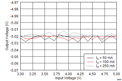
| VI = 3.7 V | ||
| VI = 3.7 V, IPOS = INEG = 100 mA | ||
| VI = 3.7 V, IPOS = INEG = 100 mA | ||

| VI = 3.7 V, IPOS = 100 mA | ||
| VI = 3.7 V to 4.2 V, IPOS = 50 mA | ||
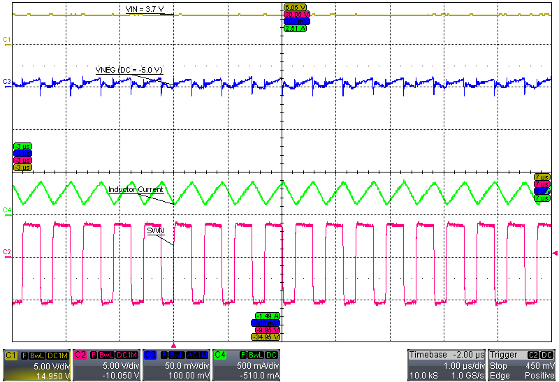
| VI = 3.7 V, INEG = 100 mA | ||
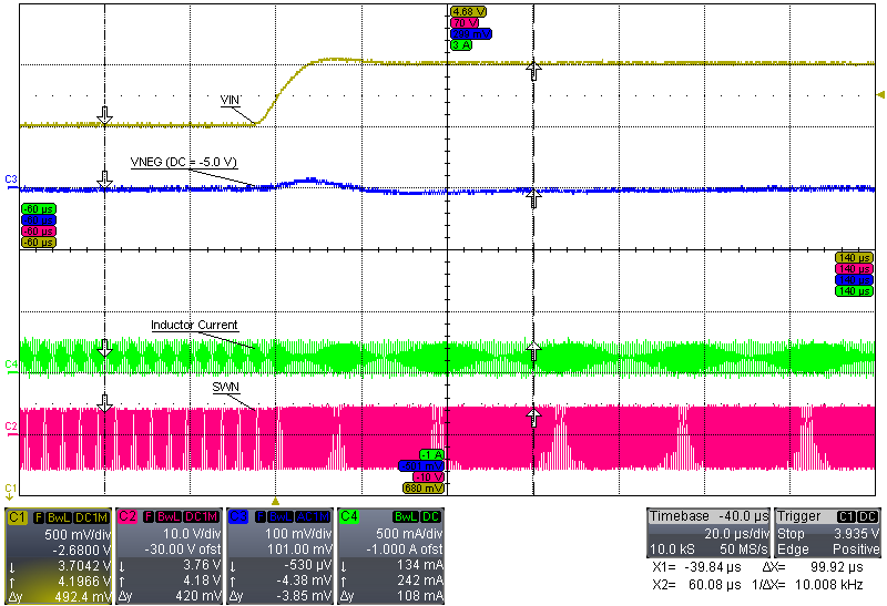
| VI = 3.7 V to 4.2 V, INEG = 50 mA | ||
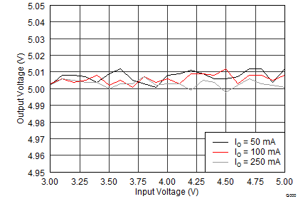
| VI = 3.7 V | ||
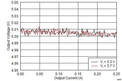

| VI = 3.7 V, IPOS = INEG = 0 mA | ||

| VI = 3.7 V, IPOS = INEG = 0 mA | ||
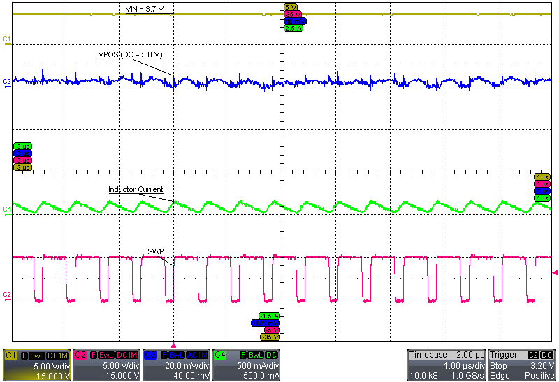
| VI = 3.7 V, IPOS = 10 mA | ||
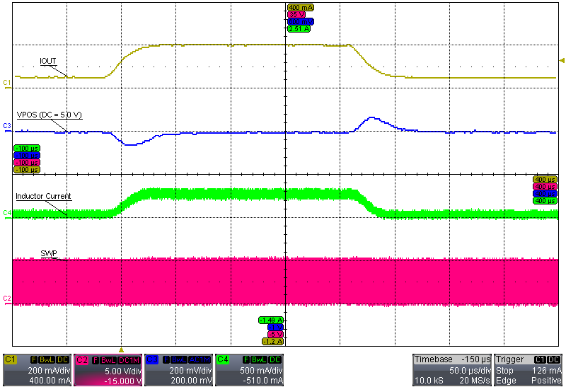
| VI = 3.7 V, IPOS = 50 mA to 200 mA | ||
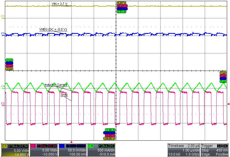
| VI = 3.7 V, INEG = 10 mA | ||
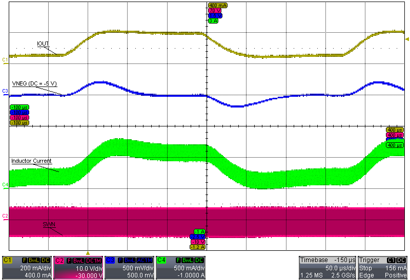
| VI = 3.7 V, INEG = 50 mA to 200 mA | ||
| IPOS = INEG = 100 mA | ||
10 Power Supply Recommendations
The TPS65133 device is designed to operate from an input supply voltage in the range 2.9 V to 5.0 V. If the input supply is located more than a few centimeters from the device additional bulk capacitance may be required. The 10-µF shown in the schematics in this data sheet are typical for this function.
11 Layout
11.1 Layout Guidelines
No PCB layout is perfect, and compromises are always necessary. However, the basic principles listed below (in order of importance) go a long way to achieving the full performance of the TPS65133 device.
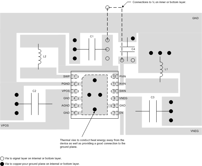
- Route discontinuous switching currents on the top layer using short, wide traces. Avoid routing these signals through vias, which have relatively high parasitic inductance and resistance.
- Place C1 as close as possible to pin 12.
- Place C2 as close as possible to pin 3. Place C3 as close as possible to pin 9.
- Use the exposed thermal pad to connect GND, AGND and PGND.
- Use a copper pour (preferably on layer 2) as a thermal spreader and connect it to the exposed thermal pad using a number of thermal vias.
Figure 28 illustrates how a PCB layout following the above principles may be realized in practice.
12 Device and Documentation Support
12.1 Device Support
12.1.1 Third-Party Products Disclaimer
TI'S PUBLICATION OF INFORMATION REGARDING THIRD-PARTY PRODUCTS OR SERVICES DOES NOT CONSTITUTE AN ENDORSEMENT REGARDING THE SUITABILITY OF SUCH PRODUCTS OR SERVICES OR A WARRANTY, REPRESENTATION OR ENDORSEMENT OF SUCH PRODUCTS OR SERVICES, EITHER ALONE OR IN COMBINATION WITH ANY TI PRODUCT OR SERVICE.
12.2 Community Resources
The following links connect to TI community resources. Linked contents are provided AS IS by the respective contributors. They do not constitute TI specifications and do not necessarily reflect TI's views; see TI's Terms of Use.
-
TI E2E™ Online Community TI's Engineer-to-Engineer (E2E) Community. Created to foster collaboration among engineers. At e2e.ti.com, you can ask questions, share knowledge, explore ideas and help solve problems with fellow engineers.
-
Design Support TI's Design Support Quickly find helpful E2E forums along with design support tools and contact information for technical support.
12.3 Trademarks
E2E is a trademark of Texas Instruments.
All other trademarks are the property of their respective owners.
12.4 Electrostatic Discharge Caution

These devices have limited built-in ESD protection. The leads should be shorted together or the device placed in conductive foam during storage or handling to prevent electrostatic damage to the MOS gates.
12.5 Glossary
SLYZ022 — TI Glossary.
This glossary lists and explains terms, acronyms, and definitions.
13 Mechanical, Packaging, and Orderable Information
The following pages include mechanical, packaging, and orderable information. This information is the most current data available for the designated devices. This data is subject to change without notice and revision of this document. For browser-based versions of this data sheet, refer to the left-hand navigation.
IMPORTANT NOTICE
Texas Instruments Incorporated and its subsidiaries (TI) reserve the right to make corrections, enhancements, improvements and other changes to its semiconductor products and services per JESD46, latest issue, and to discontinue any product or service per JESD48, latest issue. Buyers should obtain the latest relevant information before placing orders and should verify that such information is current and complete. All semiconductor products (also referred to herein as "components") are sold subject to TI's terms and conditions of sale supplied at the time of order acknowledgment.
TI warrants performance of its components to the specifications applicable at the time of sale, in accordance with the warranty in TI's terms and conditions of sale of semiconductor products. Testing and other quality control techniques are used to the extent TI deems necessary to support this warranty. Except where mandated by applicable law, testing of all parameters of each component is not necessarily performed.
TI assumes no liability for applications assistance or the design of Buyers' products. Buyers are responsible for their products and applications using TI components. To minimize the risks associated with Buyers' products and applications, Buyers should provide adequate design and operating safeguards.
TI does not warrant or represent that any license, either express or implied, is granted under any patent right, copyright, mask work right, or other intellectual property right relating to any combination, machine, or process in which TI components or services are used. Information published by TI regarding third-party products or services does not constitute a license to use such products or services or a warranty or endorsement thereof. Use of such information may require a license from a third party under the patents or other intellectual property of the third party, or a license from TI under the patents or other intellectual property of TI.
Reproduction of significant portions of TI information in TI data books or data sheets is permissible only if reproduction is without alteration and is accompanied by all associated warranties, conditions, limitations, and notices. TI is not responsible or liable for such altered documentation. Information of third parties may be subject to additional restrictions.
Resale of TI components or services with statements different from or beyond the parameters stated by TI for that component or service voids all express and any implied warranties for the associated TI component or service and is an unfair and deceptive business practice. TI is not responsible or liable for any such statements.
Buyer acknowledges and agrees that it is solely responsible for compliance with all legal, regulatory and safety-related requirements concerning its products, and any use of TI components in its applications, notwithstanding any applications-related information or support that may be provided by TI. Buyer represents and agrees that it has all the necessary expertise to create and implement safeguards which anticipate dangerous consequences of failures, monitor failures and their consequences, lessen the likelihood of failures that might cause harm and take appropriate remedial actions. Buyer will fully indemnify TI and its representatives against any damages arising out of the use of any TI components in safety-critical applications.
In some cases, TI components may be promoted specifically to facilitate safety-related applications. With such components, TI's goal is to help enable customers to design and create their own end-product solutions that meet applicable functional safety standards and requirements. Nonetheless, such components are subject to these terms.
No TI components are authorized for use in FDA Class III (or similar life-critical medical equipment) unless authorized officers of the parties have executed a special agreement specifically governing such use.
Only those TI components which TI has specifically designated as military grade or "enhanced plastic" are designed and intended for use in military/aerospace applications or environments. Buyer acknowledges and agrees that any military or aerospace use of TI components which have not been so designated is solely at the Buyer's risk, and that Buyer is solely responsible for compliance with all legal and regulatory requirements in connection with such use.
TI has specifically designated certain components as meeting ISO/TS16949 requirements, mainly for automotive use. In any case of use of non-designated products, TI will not be responsible for any failure to meet ISO/TS16949.
Products
- Audio: www.ti.com/audio
- Amplifiers: amplifier.ti.com
- Data Converters: dataconverter.ti.com
- DLP® Products: www.dlp.com
- DSP: dsp.ti.com
- Clocks and Timers: www.ti.com/clocks
- Interface: interface.ti.com
- Logic: logic.ti.com
- Power Mgmt: power.ti.com
- Microcontrollers: microcontroller.ti.com
- RFID: www.ti.rfid.com
- OMAP Application Processors: www.ti.com/omap
- Wireless Connectivity: www.ti.com/wirelessconnectivity
Applications
- Automotive and Transportation: www.ti.com/automotive
- Communications and Telecom: www.ti.com/communications
- Computers and Peripherals: www.ti.com/computers
- Consumer Electronics: www.ti.com/consumer-apps
- Energy and Lighting: www.ti.com/energy
- Industrial: www.ti.com/industrial
- Medical: www.ti.com/medical
- Security: www.ti.com/security
- Space, Avionics and Defense: www.ti.com/space-avionics-defense
- Video & Imaging: www.ti.com/video
TI E2E Community : e2e.ti.com
Mailing Address: Texas Instruments, Post Office Box 655303, Dallas, Texas 75265
Copyright© 2014, Texas Instruments Incorporated
