-
TPS65142 LCD Bias Power Integrated with WLED Backlight Drivers
- 1 Features
- 2 Applications
- 3 Description
- 4 Revision History
- 5 Pin Configuration and Functions
- 6 Specifications
-
7 Detailed Description
- 7.1 Overview
- 7.2 Functional Block Diagram
- 7.3
Feature Description
- 7.3.1 AVDD Boost Regulator
- 7.3.2 Regulated Positive Charge Pump
- 7.3.3 Negative Charge Pump
- 7.3.4 Gate Voltage Shaping
- 7.3.5 VCOM Buffer
- 7.3.6 Reset
- 7.3.7 Under-voltage Lockout (UVLO)
- 7.3.8 Thermal Shutdown
- 7.3.9 WLED Boost Regulator
- 7.3.10 Current Sinks
- 7.3.11 Unused IFB Pins
- 7.3.12 PWM Dimming
- 7.3.13 Enabling the WLED Driver
- 7.3.14 Soft-Start of WLED Boost Regulator
- 7.3.15 Protection of WLED Driver
- 7.3.16 Power Up/Down Sequence
- 8 Application and Implementation
- 9 Device and Documentation Support
- 10Mechanical, Packaging, and Orderable Information
- IMPORTANT NOTICE
Package Options
Mechanical Data (Package|Pins)
- RTG|32
Thermal pad, mechanical data (Package|Pins)
- RTG|32
Orderable Information
TPS65142 LCD Bias Power Integrated with WLED Backlight Drivers
1 Features
- Integrated Bias and Backlight Power
- 2.3-V to 6-V Input Voltage Range for Bias
- Up to 16.5 V Boost Converter with 1.8-A Switch Current
- 1.2-MHz / 650-kHz Selectable Switching Frequency
- Internal Compensation
- Internal Soft-start at Power on
- Reset Function (XAO Signal)
- Regulated VGH
- Regulated VGL
- Gate Voltage Shaping
- LCD Discharge Function
- 150-mA Unity Gain VCOM Buffer
- 4.5-V to 24-V WLED Backlight Input Range
- Integrated 1.5-A / 40-V MOSFET
- Boost Output Tracks WLED Voltage
- Internal Compensation
- External Current Setting Input
- 6 Current-Sink Channels of 25 mA
- Better than 3% Current Matching
- Up to 1000:1 PWM Dimming Range
- Overvoltage Protection
- Thermal Shutdown
- Undervoltage Lockout
- 32-Pin 6 mm × 3 mm QFN Package
2 Applications
- Note-PC TFT-LCD Panels
- Tablet TFT-LCD Panels
3 Description
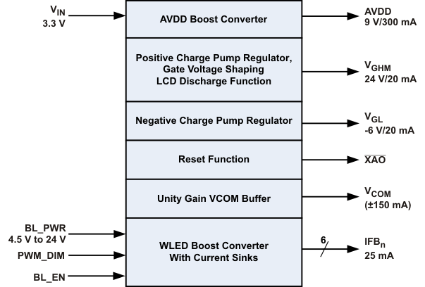
The TPS65142 provides a compact solution to the bias power and the WLED backlight in note-pc TFT-LCD panels. The device features a boost converter, a positive charge pump regulator, and a negative charge pump regulator to power the source drivers and the gate drivers. A 150 mA unity-gain high-speed buffer is offered to drive the VCOM plane. Gate voltage shaping and the LCD discharge function are offered to improve the image quality. A reset function allows a proper reset of the TCON at the power on. The TPS65142 also offers the complete solution to driver up to 6 chains of WLEDs with 1000:1 ratio PWM dimming.
All features are integrated in a compact 6 x 3 mm2 Thin QFN package.
Device Information(1)
| PART NUMBER | PACKAGE | BODY SIZE (NOM) |
|---|---|---|
| TPS65142 | WQFN (32) | 6.00 mm x 3.00 mm |
- For all available packages, see the orderable addendum at the end of the data sheet.
Simplified Block Diagram
4 Revision History
Changes from A Revision (November 2012) to B Revision
- Added the ESD Ratings table, Feature Description, Application and Implementation, Power Supply Recommendations, Device and Documentation Support, and Mechanical, Packaging, and Orderable InformationGo
- Deleted the Ordering Information table Go
- Added Timing Requirements table. Go
- Added sentence to the Power Up Sequence section: "To ensure proper start-up..."Go
- Changed Figure 32Go
Changes from * Revision (July 2011) to A Revision
- Deleted COMP pin from ABSOLUTE MAXIMUM RATINGSGo
- Changed I(IFB_MAX) TEST CONDITION IFB from 450 mV to 500 mVGo
- Changed I(IFB_MAX) min from 25 mA to 28 mAGo
- Changed Dmax min from 85% to 89%Go
- Changed VREF from 3.15 V to 3.12 V in Negative Charge Pump sectionGo
- Changed BL_PWR from 4.5V to 25V to 4.5V to 24V in Figure 33Go
5 Pin Configuration and Functions
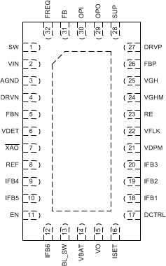
Pin Functions
| PIN | I/O | DESCRIPTION | |
|---|---|---|---|
| NAME | NO. | ||
| AGND | 3 | Analog ground | |
| BL_SW | 13 | The backlight boost converter switching node | |
| DCTRL | 17 | I | Backlight PWM dimming control input |
| DRVN | 4 | O | Voltage driver of the negative charge pump |
| DRVP | 27 | Voltage driver of positive charge pump | |
| EN | 11 | I | Backlight enable input |
| FB | 31 | I | AVDD Boost converter feedback pin |
| FBN | 5 | I | Negative charge pump feedback pin |
| FBP | 26 | I | Positive charge pump feedback pin |
| FREQ | 32 | I | AVDD boost converter switching frequency selection: 1.2MHz when V(FREQ) = VIN and 650 kHz when V(FREQ) = ground |
| IFB1 | 18 | I | Channel 1 of the WLED backlight current sink |
| IFB2 | 19 | I | Channel 2 of the WLED backlight current sink |
| IFB3 | 20 | I | Channel 3 of the WLED backlight current sink |
| IFB4 | 9 | I | Channel 4 of the WLED backlight current sink |
| IFB5 | 10 | I | Channel 5 of the WLED backlight current sink |
| IFB6 | 12 | I | Channel 6 of the WLED backlight current sink |
| ISET | 16 | I | WLED current sink level programming input |
| OPI | 30 | I | Input voltage of VCOM Buffer |
| OPO | 29 | O | Output voltage of VCOM Buffer |
| PGND | ePAD | Exposed pad that serves as the power ground for both boost converters | |
| RE | 23 | Sets the slope for the gate shaping function. Pin for external Resistor | |
| REF | 8 | O | Reference voltage for the negative charge pump |
| SUP | 28 | I | Supply pin of the gate shaping and operational amplifier blocks. Connected as well to the overvoltage protection comparator. This pin needs to be connected to the output of the AVDD boost converter. |
| SW | 1 | Switch pin of the AVDD boost converter | |
| VBAT | 14 | I | Input of the backlight boost converter |
| VDET | 6 | I | Reset IC threshold pin (Voltage divider) |
| VDPM | 21 | O | Sets the delay to enable VGHM Output. Pin for external capacitor. Floating if no delay needed |
| VFLK | 22 | I | Charge/discharge signal for VGHM |
| VGH | 25 | I | Input for positive Charge Pump |
| VGHM | 24 | O | Output for gate-high modulation |
| VIN | 2 | I | Input supply pin |
| VO | 15 | O | The output of the backlight boost converter |
| XAO | 7 | O | Reset IC output pulling down XAO pin when active. |
6 Specifications
Absolute Maximum Ratings(1)
over operating free-air temperature range (unless otherwise noted)6.1 ESD Ratings
| VALUE | UNIT | |||
|---|---|---|---|---|
| V(ESD) | Electrostatic discharge | Human-body model (HBM), per ANSI/ESDA/JEDEC JS-001(1) | ±2000 | V |
| Charged-device model (CDM), per JEDEC specification JESD22-C101(2) | ±500 | |||
6.2 Recommended Operating Conditions
| MIN | TYP | MAX | UNIT | ||
|---|---|---|---|---|---|
| VIN | Input voltage range | 2.3 | 6 | V | |
| VS | AVDD Boost output voltage range(1) | 16.5 | V | ||
| VGH | Positive charge pump output voltage range | 32 | V | ||
| VBAT | Battery voltage range | 4.5 | 24 | V | |
| VO | WLED boost converter output voltage | 38 | V | ||
| VGL | Negative charge pump output voltage range | –14 | V | ||
| L1 | Inductor for the AVDD boost converter(2) | 4.7 | 10 | µH | |
| L2 | Inductor for the WLED boost converter | 4.7 | 10 | µH | |
| CIN | Input decoupling capacitor | 1 | µF | ||
| CO1 | Output decoupling capacitor of the AVDD boost converter | 20 | µF | ||
| CO2 | Output decoupling capacitor of the WLED boost converter | 2.2 | 10 | µF | |
| TA | Operating ambient temperature | –40 | 85 | °C | |
| TJ | Operating junction temperature | –40 | 125 | °C |
6.3 Thermal Information
| THERMAL METRIC(1) | WQFN | UNITS | |
|---|---|---|---|
| RTG (32 PINS) | |||
| RθJA | Junction-to-ambient thermal resistance | 35.4 | °C/W |
| RθJCtop | Junction-to-case (top) thermal resistance | 19.9 | |
| RθJB | Junction-to-board thermal resistance | 5.6 | |
| ψJT | Junction-to-top characterization parameter | 0.2 | |
| ψJB | Junction-to-board characterization parameter | 5.4 | |
| RθJCbot | Junction-to-case (bottom) thermal resistance | 1.7 | |
6.4 Electrical Characteristics
VIN = 3.3 V, VS = 9V, VGH = 20 V, VBAT = 10.8V, IISET = 15µA, VIFBx = 0.5V, EN = VIN, TA = –40°C to 85°C, typical values are at TA = 25°C (unless otherwise noted)| PARAMETER | TEST CONDITIONS | MIN | TYP | MAX | UNIT | |
|---|---|---|---|---|---|---|
| SUPPLY | ||||||
| IQ(IN) | Operating quiescent current into VIN | Device not switching | 0.17 | 0.5 | mA | |
| IQ(VGH) | Operating quiescent current into VGH | VGH = 20 V, VFLK not oscillating | 22 | 40 | µA | |
| IQ(SUP) | Operating quiescent current into SUP | Device not switching. VS = 9 V, EN = high | 2.8 | mA | ||
| Device not switching. VS = 9 V, EN = GND | 2.5 | |||||
| ISD(VIN) | Shutdown current into VIN | VIN = 1.8 V, VS = GND | 20 | 33 | µA | |
| ISD(VGH) | Shutdown current into VGH | VIN = 1.8 V, VGH = 32 V | 30 | 50 | µA | |
| ISD(SUP) | Shutdown current into SUP | VIN = 1.8 V, VS = 16.5 V | 3 | 5 | µA | |
| IQ(BAT) | VBAT pin quiescent current | WLED boost regulator switching, no load | 0.2 | mA | ||
| ISD(BAT) | VBAT pin shutdown current | EN = GND | 18 | µA | ||
| IQ(VO) | VO pin quiescent current | VO = 35 V | 75 | µA | ||
| UVLO | VIN under voltage lockout threshold | VIN falling | 1.9 | 2.1 | V | |
| VIN rising | 2.2 | |||||
| VBAT under voltage lockout threshold | VBAT rising | 4.45 | V | |||
| VBAT falling | 3.9 | |||||
| UVLO voltage of WLED control circuit | 2.2 | 2.5 | V | |||
| LOGIC SIGNALS FREQ, VFLK, EN, DCTRL | ||||||
| VIH | Logic high input voltage | VIN = 2.5 V to 6 V | 2 | V | ||
| VIL | Logic low input voltage | VIN = 2.5 V to 6 V | 0.5 | V | ||
| ILKG | Input leakage current of VFLK pin | VFLK = 6 V, FREQ = GND | 0.1 | µA | ||
| RPD | Pull-down resistance for EN and DCTRL pins | EN = DCTRL = 3.3 V | 400 | 800 | 1600 | kΩ |
| AVDD BOOST CONVERTER | ||||||
| VS | Output voltage boost(1) | 7 | 16.5 | V | ||
| VOVP | Overvoltage protection | VS rising | 16.9 | 18 | 19 | V |
| VFB | Feedback regulation voltage | TA = –40°C to 85°C | 1.226 | 1.24 | 1.254 | V |
| TA = 25°C | 1.23 | 1.24 | 1.25 | |||
| IFB | Feedback input bias current | VFB = 1.240 V | 0.1 | µA | ||
| rDS(ON) | N-channel MOSFET on-resistance | VIN = VGS = 5 V, ISW = current limit | 0.13 | 0.38 | Ω | |
| VIN = VGS = 3.3 V, ISW = current limit | 0.15 | 0.44 | ||||
| ILkg(SW) | AVDD Boost converter SW leakage current | VIN = 1.8 V, VSW = 17 V, Device not switching | 30 | µA | ||
| ILIM | N-Channel MOSFET current limit | VIN = 2.5 V to 6 V | 1.8 | 2.5 | 3.2 | A |
| VIN = 2.3 V to 2.5 V | 1.5 | A | ||||
| fBOOST | Switching frequency | FREQ = high | 0.9 | 1.2 | 1.5 | MHz |
| FREQ = low | 470 | 625 | 780 | kHz | ||
| TSS | Softstart time | FREQ = high, L1 = 6.8 µH, CO1 = 2 0µF and 10 mA load current |
2 | ms | ||
| Line regulation | VIN = 2.5 V … 6 V, IOUT = 10 mA | 0.008 | %/V | |||
| Load regulation | IOUT = 0 mA …500 mA | 0.15 | %/A | |||
| VGH REGULATOR | ||||||
| fSWP | Switching frequency | 0.5 x fBOOST | MHz | |||
| VFBP | Reference voltage of feedback | TA = –40°C to 85°C | 1.210 | 1.240 | 1.270 | V |
| TA = 25°C | 1.221 | 1.240 | 1.259 | |||
| IFBP | Feedback input bias current | VFBP = 1.240 V | 0.1 | µA | ||
| rDS(ON)P1 | DRVP RDS(ON) (PMOS) | VS = 9 V, I(DRVP) = 40 mA | 8 | 20 | Ω | |
| rDS(ON)N1 | DRVP RDS(ON) (NMOS) | VS = 9 V, I(DRVP) = –40 mA | 3 | 10 | Ω | |
| VGL REGULATOR | ||||||
| fSWN | Switching frequency | 0.5 x fBOOST | MHz | |||
| VREF | Reference voltage | 3.05 | 3.12 | 3.18 | V | |
| VFBN | Reference voltage of feedback | –48 | 0 | 48 | mV | |
| IFBN | Feedback input bias current | VFBN = 0 V | 0.1 | µA | ||
| rDS(ON)P2 | DRVN RDS(ON) (PMOS) | VS = 9 V, I(DRVN) = 40 mA | 8 | 20 | Ω | |
| rDS(ON)N2 | DRVN RDS(ON) (NMOS) | VS = 9 V, I(DRVN) = –40 mA | 3 | 10 | Ω | |
| GATE VOLTAGE SHAPING VGHM | ||||||
| I(DPM) | Capacitor charge current VDPM pin | 17 | 20 | 23 | µA | |
| rDS(ON)M1 | VGH to VGHM rDS(ON) (M1 PMOS) | VFLK = low, I(VGHM) = 20 mA | 13 | 25 | Ω | |
| rDS(ON)M2 | VGHM to RE rDS(ON) (M2 PMOS) | VFLK = high, I(VGHM) = 20 mA, VGHM = 7.5 V | 13 | 25 | Ω | |
| RESET | ||||||
| VIN(DET) | VIN voltage range for reset detection | 1.6 | 6 | V | ||
| V(DET) | Reset IC threshold | Falling | 1.074 | 1.1 | 1.126 | V |
| V(DET_HYS) | Reset IC threshold hysteresis | 65 | mV | |||
| I(DET_B) | Reset IC input bias current | V(DET) = 1.1 V | 0.1 | µA | ||
| IXAO | Reset sink current capability(2) | V(XAO_ON) = 0.5 V | 1 | mA | ||
| ILKG(XAO) | Reset leakage current | V(XAO) = VIN = 3.3 V | 2 | µA | ||
| VCOM BUFFER | ||||||
| VSUP | SUP input supply range(3) | 7 | 16.5 | V | ||
| IB | Input bias current | VCM = V(OPI) = VSUP/2 = 4.5 V | –1 | 1 | µA | |
| VCM | Common Mode Input Voltage Range | VOFFSET = 10 mV, I(OPO) = 10 mA | 2 | VS – 2 | V | |
| CMRR | Common Mode Rejection Ratio(4) | VCM = V(OPI) = V(SUP)/2 = 4.5 V, 1 MHz | 66 | dB | ||
| AVOL | Open Loop Gain(4) | VCM = V(OPI) = V(SUP)/2 = 4.5 V, no load | 90 | dB | ||
| VOL | Output Voltage Swing Low | I(OPO) = 10 mA | 0.10 | 0.25 | V | |
| VOH | Output Voltage Swing High | I(OPO) = 10 mA | VS – 0.8 | VS – 0.65 | V | |
| ISC | Short Circuit Current | Source (V(OPI) = 4.5V, V(OPO) = GND) | 150 | mA | ||
| Sink (V(OPI) = 4.5 V, V(OPO) = 9 V) | 150 | |||||
| IO | Output Current | Source (V(OPI) = 4.5 V, V(OFFSET) = 15 mV) | 150 | mA | ||
| Sink (V(OPI) = 4.5 V, V(OFFSET) = 15 mV) | 140 | |||||
| PSRR | Power Supply Rejection Ratio(4) | 40 | dB | |||
| SR | Slew Rate(4) | AV = 1, V(OPI) = 2 VPP | 40 | V/µs | ||
| BW | –3 dB Bandwidth(4) | AV = 1, V(OPI) = 60 mVPP | 50 | MHz | ||
| WLED CURRENT REGULATION | ||||||
| V(ISET) | ISET pin voltage | 1.204 | 1.229 | 1.253 | V | |
| K(ISET) | Current multiple IOUT/ISET (5) | ISET current = 20 µA | 1000 | |||
| IFB | Current accuracy (5) | ISET current = 20 µA | 19.4 | 20 | 20.6 | mA |
| Km | (Imax–Imin)/IAVG | ISET current = 20 µA | 1% | 2.5% | ||
| ILKG | IFB pin leakage current | IFB voltage = 20 V on all pins | 3 | µA | ||
| I(IFB_MAX) | Current sink max output current | IFB = 500 mV | 28 | mA | ||
| WLED BOOST OUTPUT REGULATION | ||||||
| V(IFB_L) | VO dial up threshold | Measured on V(IFB) min | 400 | mV | ||
| V(IFB_H) | VO dial down threshold | Measured on V(IFB) min | 700 | mV | ||
| V(reg_L) | Minimum VO regulation voltage | 16 | V | |||
| VO(step) | VO stepping voltage | 100 | 150 | mV | ||
| WLED BOOST REGULATOR POWER SWITCH | ||||||
| R(PWM_SW) | PWM FET on-resistance | 0.2 | 0.45 | Ω | ||
| I(LN_NFET) | PWM FET leakage current | V(BL_SW) = 35 V, TA = 25°C | 1 | µA | ||
| WLED OSCILLATOR | ||||||
| fS | Oscillator frequency | 0.9 | 1.0 | 1.2 | MHz | |
| Dmax | Maximum duty cycle of WLED Boost | IFB = 0 V | 89% | 94% | ||
| Dmin | Minimum duty cycle of WLED Boost | 7% | ||||
| CURRENT LIMIT, OVER VOLTAGE AND SHORT CIRCUIT PROTECTIONS | ||||||
| ILIM | N-Channel MOSFET current limit | D = DMAX | 1.5 | 3 | A | |
| VOVP | VO overvoltage threshold | Measured on the VO pin | 38 | 39 | 40 | V |
| VOVP(IFB) | IFB overvoltage threshold | Measured on the IFBx pin | 15 | 17 | 20 | V |
| VSC | Short circuit detection threshold | VBAT –VO, VO ramp down | 1.7 | 2.5 | V | |
| VSC(dly) | Short circuit detection delay during start up | 32 | ms | |||
| THERMAL SHUTDOWN | ||||||
| TSD | Thermal shutdown | Temperature rising | 150 | °C | ||
| TSDHYS | Thermal shutdown hysteresis | 14 | °C | |||
6.5 Timing Requirements
| MIN | NOM | MAX | UNIT | ||
|---|---|---|---|---|---|
| td | Rising edge delay between VBAT and VIN, measured at their respective rising edge UVLO threshold voltages (see Figure 32). (1) | 0 | s | ||
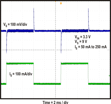
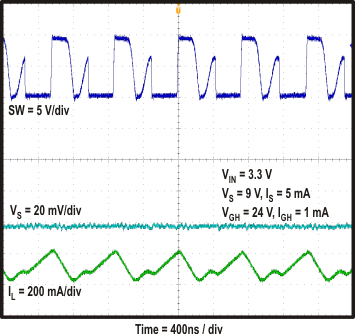
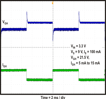
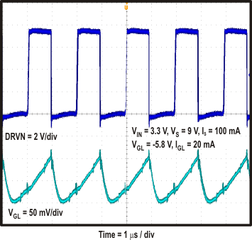
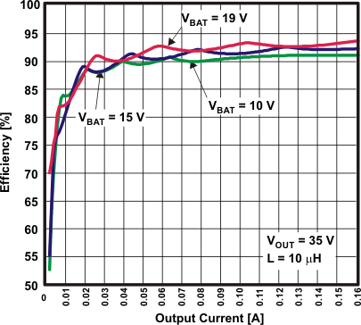
6.6 Typical Characteristics




7 Detailed Description
7.1 Overview
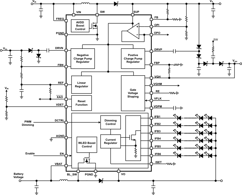
The TPS65142 offers a compact and complete solution to the bias power and the WLED backlight in note-pc TFT-LCD panels. The device features an AVDD boost regulator, a positive charge pump regulator, and a negative charge pump regulator to power the source drivers and the gate drivers. A 150-mA unity-gain high-speed buffer is provided to drive the VCOM plane. Gate voltage shaping and the LCD discharge function are offered to improve the image quality. A reset function allows a proper reset of the TCON at power on or the gate driver ICs during power off. The TPS65142 also includes the complete solution to drive up to 6 chains of WLEDs with 1000:1 ratio PWM dimming.
7.2 Functional Block Diagram
7.3 Feature Description
7.3.1 AVDD Boost Regulator
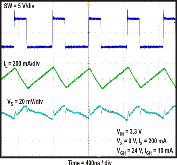
The AVDD boost regulator is designed for output voltages up to 16.5 V with a switch peak current limit of 1.8 A minimum. The device, which operates in a current-mode scheme with quasi-constant frequency, is internally compensated to minimize the pin and component counts. The switching frequency is selectable between 650 kHz and 1.2 MHz and the minimum input voltage is 2.3 V.
During the on-time, the current rises in the inductor. When the current reaches a threshold value set by the internal GM amplifier, the power transistor is turned off. The polarity of the inductor voltage changes and forward biases the Schottky diode, which lets the current flow towards the output of the boost regulator. The off-time is fixed for a certain input voltage VIN and output voltage VS, and therefore maintains the same frequency when varying these parameters. However, for different output loads, the frequency changes slightly due to the voltage drop across the rDS(on) of the power transistor which will have an effect on the voltage across the inductor and thus on tON (tOFF remains fixed).
The fixed off-time maintains a quasi-fixed frequency that provides better stability for the system over a wide range of input and output voltages than conventional boost converters. The TPS65142 topology has also the benefits of providing very good load and line regulations, and excellent line and load transient responses.
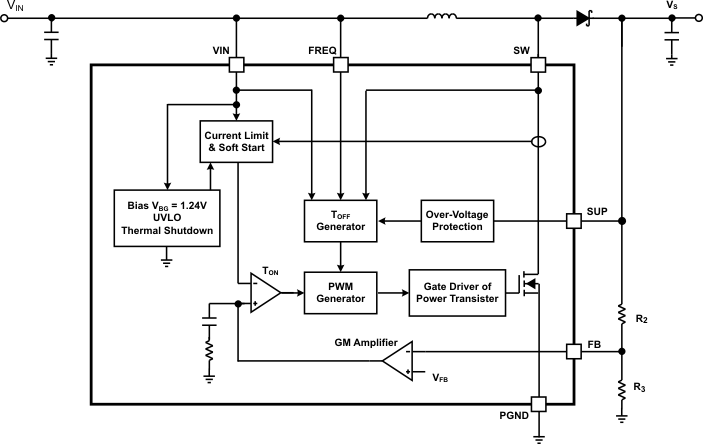 Figure 25. Boost Converter Block Diagram
7.3.1.1 Setting the Output Voltage
The output voltage is set by an external resistor divider. Typically, a minimum current of 50 µA flowing through the feedback divider is enough to cover the noise fluctuation. If 70 µA is chosen for higher noise immunity, the resistors shown in Figure 25 are then calculated as:

where VFBP = 1.240 V
7.3.1.2 Soft-Start (AVDD Boost Converter)
The AVDD boost converter has an internal digital soft-start to prevent high inrush current during start-up. The typical soft-start time is 2 ms.
7.3.1.3 Frequency Select Pin (FREQ)
The digital frequency-select pin FREQ allows to set the switching frequency of the device to 650 kHz (FREQ = low) or 1.2 MHz (FREQ = high). Higher switching frequency improves load transient response but reduces slightly the efficiency. The other benefit of a higher switching frequency is the lower output voltage ripple. Usually, it is recommended to use 1.2-MHz switching frequency unless light load efficiency is a major concern.
7.3.1.4 Overvoltage Protection
The AVDD boost converter has an integrated over-voltage protection to prevent the power switch from exceeding the absolute maximum switch voltage rating at pin SW in case the feedback (FB) pin is floating or shorted to GND. In such an event, the output voltage rises and is monitored with the overvoltage protection comparator over the SUP pin. As soon as the comparator trips at typically 18 V, the boost converter turns the N-Channel MOSFET switch off. The output voltage falls below the overvoltage threshold and the converter continues to operate. In order to detect overvoltage, the SUP pin must to be connected to the output voltage of the boost converter VS.
7.3.2 Regulated Positive Charge Pump
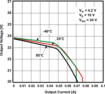
The positive charge pump sets the voltage applied on the VGH input pin, up to 32 V in tripler mode configuration. The charge pump block regulates the VGH voltage by adjusting the drive current IDRVP. Typically, a minimum current of 50 µA flowing through the feedback divider is usually enough to cover the noise fluctuation. If 70 µA is chosen for higher noise immunity, the resistors of the divider used to set the VGH voltage are calculated as (refer to Figure 26):

where VFBP = 1.240 V
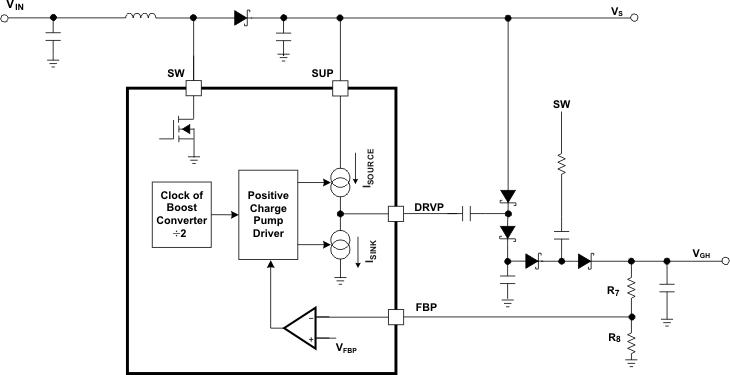 Figure 26. Block Diagram of the Positive Charge Pump Regulator
7.3.3 Negative Charge Pump
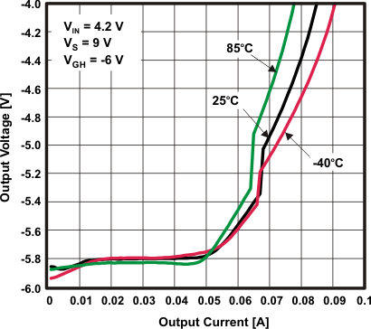
Figure 27 shows the block diagram of the negative charge pump. The negative charge pump needs to generate a voltage of –6 V to –7 V with a negative inverter or –12 V to –13 V with a negative doubler. The reference voltage from the REF pin is 3.15 V. The bias to the REF block comes from the SUP pin. The error amplifier is referenced to the ground. The VGL can be set with the following equation:

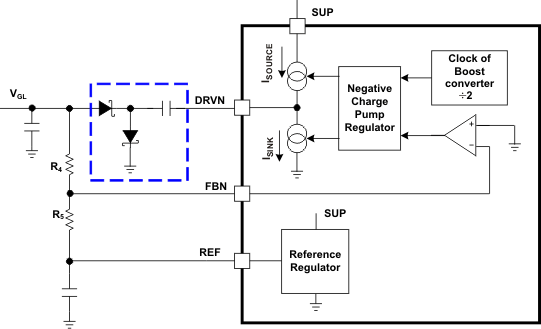 Figure 27. Block Diagram of the Negative Charge Pump Regulator with a Negative Inverter Configuration
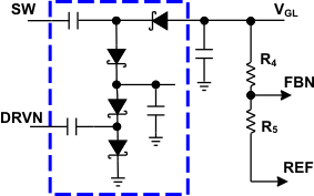 Figure 28. Negative Doubler Configuration for the Negative Charge Pump Regulator
7.3.4 Gate Voltage Shaping
The VGHM output is controlled by the VFLK logic input and the VDPM voltage level.
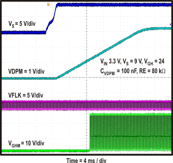
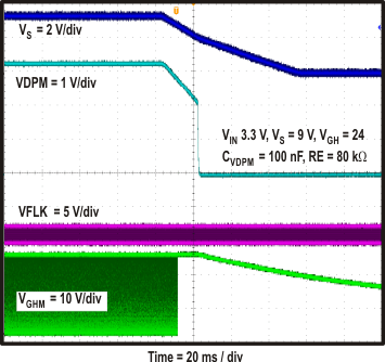
The VDPM pin allows the user to set a delay before the Gate Voltage Shaping starts. The voltage of the VDPM pin is zero volt at power on. When the output voltage of the AVDD boost converter rises above a power-good threshold, a power-good signal enables a 20-µA current source that charges the capacitor connected between the VDPM pin and the ground. When the VDPM-pin voltage rises to 1.24 V, the Gate Voltage Shaping is enabled.
The VFLK input controls the M1 and the M2 transistors, as shown in Figure 29, after the Gate Voltage Shaping is enabled:
When VFLK = “low”, M1 is turned on so VGHM is connected to the VGH input.
When VFLK = “high”, M2 is turned on so VGHM voltage is discharged through M2 and the resistor connected to the RE pin.
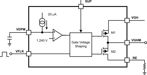 Figure 29. Block Diagram of the Gate Voltage Shaping Function
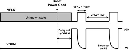 Figure 30. Gate Voltage Shaping Timing
7.3.5 VCOM Buffer
The VCOM Buffer power supply pin is the SUP pin connected to the AVDD boost converter VS. To achieve good performance and minimize the output noise, a 1-µF ceramic bypass capacitor is required directly from the SUP pin to ground. The buffer is not designed to drive high capacitive loads; therefore, it is recommended to connect a series resistor at the output to provide stable operation when driving a high capacitive load. With a 3.3-Ω series resistor, a capacitive load of 10 nF can be driven, which is usually sufficient for typical LCD applications.
7.3.6 Reset
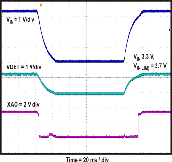
The device has an integrated reset function with an open-drain output capable of sinking 1 mA. The reset function monitors the voltage applied to its sense input V(DET). As soon as the voltage on V(DET) falls below the threshold voltage, V(DET), of typically 1.1 V, the reset function asserts its reset signal by pulling XAO low. Typically, a minimum current of 50 µA flowing through the feedback divider is enough to cover the noise fluctuation. Therefore, to select R12 and R13 (see Figure 33), one has to set the input voltage limit (VIN(LIM)) at which the reset function will pull XAO to low state. VIN(LIM) must be higher than the UVLO threshold. If 70 µA is chosen,

where VDET = 1.1 V.
The XAO output is also controlled by the UVLO function. When the input voltage is below the UVLO threshold, XAO output is forced low until the input voltage is lower than 1.6 V. The XAO output is in an unknown state when the input voltage is below the 1.6 V threshold.
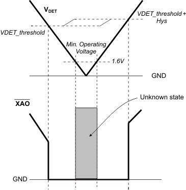 Figure 31. Voltage Detection and XAO Pin
When the input voltage VIN rises, once the voltage on VDET pin exceeds its threshold voltage plus the hysteresis, the XAO signal will go high.
The reset function is operational for VIN ≥ 1.6 V.
The reset function is configured as a standard open-drain and requires a pull-up resistor. The resistor R(XAO) (R14 in Figure 33), which must be connected between the XAO pin output and a positive voltage VX greater than 2 V – 'high' logic level can be chosen as follows:

7.3.7 Under-voltage Lockout (UVLO)
The TPS65142 monitors both VIN and VBAT inputs for under-voltage lockout. When the VIN input in under its UVLO threshold, the whole IC is disabled to avoid mis-operation. When the VIN input rises above its UVLO threshold, all functions are enabled except the WLED driver. The WLED driver, including the WLED boost converter and the current sinks, will be enabled when the VBAT input is also higher than its UVLO threshold.
7.3.8 Thermal Shutdown
A thermal shutdown is implemented to prevent damages because of excessive heat and power dissipation. Typically the thermal shutdown threshold for the junction temperature is 150°C. When the thermal shutdown is triggered the device stops switching until the junction temperature falls below typically 136°C. Then the device starts switching again.
7.3.9 WLED Boost Regulator
The WLED boost regulator is a current-mode PWM regulator with internal loop compensation. The internal compensation ensures a stable output over the full input and output voltage range. The WLED boost regulator switches at fixed 1 MHz. The output voltage of the boost regulator is automatically set by the TPS65142 to minimize the voltage drop across the current-sink IFBx pins. The lowest IFB-pin voltage to regulated to 400 mV. When the output voltage is too close to the input, the WLED boost regulator may not be able to regulate the output due to the limitation of the minimum duty cycle. In that case, the user needs to increase the number of WLED in series or to include series ballast resistors to provide enough headroom for the boost converter to operate. The WLED boost regulator cannot regulate its output to a voltage below 15 V.
7.3.10 Current Sinks
The six current sink regulators can each provide a maximum of 25 mA. The IFB current must be programmed to the highest WLED current expected using an ISET-pin resistor with the following equation:

where
K(ISET) = Current multiple (1000 typical)
V(ISET) = ISET pin voltage (1.229 V typical)
R(ISET) = ISET-pin resistor value
The TPS65142 has built-in precise current sink regulators. The current matching error among 6 current sinks is below 2.5%. This means the differential values between the maximum and minimum currents of the six current sinks divided by the average current of the six is less than 2.5%.
7.3.11 Unused IFB Pins
If the application requires less than 6 WLED strings, one can easily disable unused IFBx pins by simply leaving the unused IFB pin open or shorting it to ground. If the IFB pin is open, the boost output voltage ramps up to VO overvoltage threshold during start up. The IC then detects the zero current string and removes it from the feedback loop. If the IFB pin is shorted to ground, the IC detects the short immediately after WLED driver is enable, and the boost output voltage does not go up to VO overvoltage threshold. Instead, it ramps to the regulation voltage after the soft start.
7.3.12 PWM Dimming
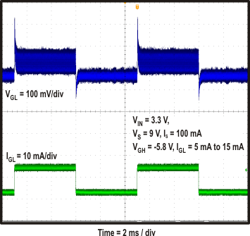
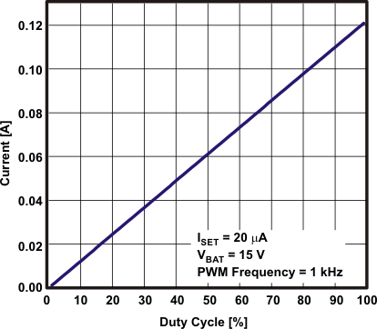
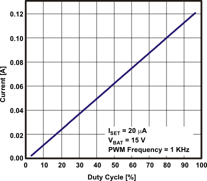
The WLED brightness is controlled by the PWM signal on the DCTRL pin. The frequency and duty cycle of the DCTRL signal is replicated on the IFB pin current. Keep the dimming frequency in the range of 100 Hz to 1 kHz to avoid screen flickering and to maintain dimming linearity. Screen flickering may occur if the dimming frequency is below the range. The minimum achievable duty cycle increases with the dimming frequency. For example, while a 0.1% dimming duty cycle, giving a 1000:1 dimming range, is achievable at 100 Hz dimming frequency, only 1% duty cycle, giving a 100:1 dimming range, is achievable with a 1-kHz dimming frequency, and 5% dimming duty cycle is achievable with 5 kHz dimming frequency. The device can work at high dimming frequency such as 20 kHz, but then only 15% duty cycle can be achieved. The TPS65142 is designed to minimize the AC ripple on the output capacitor during PWM dimming. Careful passive component selection is also critical to minimize AC ripple on the output capacitor.
7.3.13 Enabling the WLED Driver
The WLED driver (including the WLED boost converter and the six current sinks) is enabled when all following four conditions are satisfied:
- the VBAT input voltage is higher than its under-voltage-lockout (UVLO) threshold;
- the REF regulator output is higher than its power-good threshold;
- the output voltage VO is within 2 V of the input voltage VBAT;
- and the enable input from the EN pin is high.
Pulling the EN pin low shuts down the WLED driver.
7.3.14 Soft-Start of WLED Boost Regulator
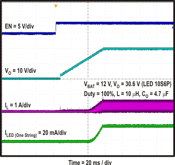
Once the above four conditions are satisfied, the WLED boost converter begins the internal soft-start. The soft-start function gradually ramps up the reference voltage of the error amplifier to prevent the output-voltage over shoot and inrush current from the VBAT input.
7.3.15 Protection of WLED Driver
The TPS65142 has multiple protection mechanisms to secure the safe operation of the WLED driver.
7.3.15.1 Current Limit Protection
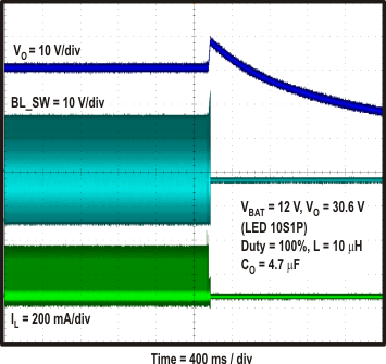
The WLED boost regulator switching MOSFET has a pulse-by-pulse over-current limit of 1.5 A (minimum value). The PWM switch turns off when the inductor current reaches this current threshold and remains off until the beginning of the next switching cycle. This protects the device and external components under over-load conditions. When there is sustained overcurrent condition for more than 16 ms (under 100% dimming duty cycle), the IC turns off and requires VBAT POR or the EN pin toggling to restart.
Under severe over load and/or short-circuit conditions, the VO pin can be pulled below the input (VBAT pin voltage). Under this condition, the current can flow directly from the input to the output through the inductor and the Schottky diode. Turning off the PWM switch alone does not limit current anymore. In this case, the TPS65142 relies on the fuse at the input to protect the whole system. When the TPS65142 detects the output voltage to be 1 V (short-circuit detection threshold) below the input voltage, it shuts down the WLED driver. The IC restarts after input power-on reset (VBAT POR) or EN pin logic toggling.
7.3.15.2 Open WLED String Protection
If one of the WLED strings is open, the boost output rises to its over-voltage threshold (39 V typically). The IC detects the open WLED string by sensing no current in the corresponding IFBx pin. As a result, the IC removes the open IFBx pin from the voltage feedback loop. The output voltage drops and is regulated to the voltage for the remaining connected WLED strings. The IFBx current of the connected WLED string remains in regulation during the whole transition.
The IC shuts down if it detects that all of the WLED strings are open.
7.3.15.3 Overvoltage Protection
If the overvoltage threshold is reached, but the current sensed on the IFBx pin is below the regulation target, the IC regulates the boost output at the overvoltage threshold. This operation could occur when the WLED is turned on under cold temperature, and the forward voltages of the WLEDs exceed the over-voltage threshold. Maintaining the WLED current allows the WLED to warm up and their forward voltages to drop below the overvoltage threshold.
If any IFBx pin voltage exceeds IFB overvoltage threshold (17 V typical), the IC turns off the corresponding current sink and removes this IFB pin from VO regulation loop. The remaining IFBx pins’ current regulation is not affected. This condition often occurs when there are several shorted WLEDs in one string. WLED mismatch typically does not create such large voltage difference among WLED strings.
7.3.16 Power Up/Down Sequence
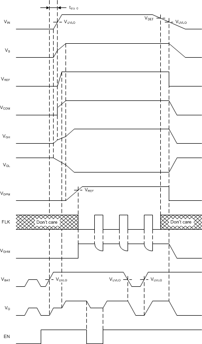
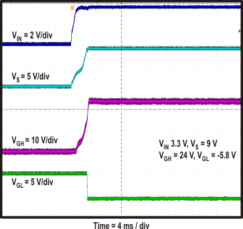
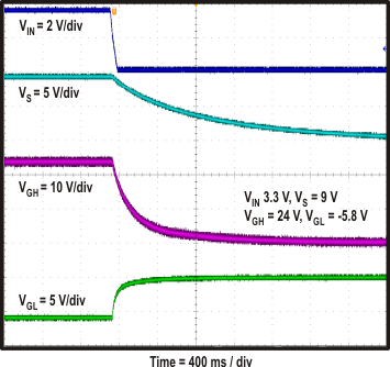
The power up and power down sequences are shown in Figure 32.
The operation of the bias converters are gated by the UVLO of the VIN voltage. The start-up of the WLED boost converter is gated by the UVLO of the VBAT input, the power good of the REF output, the (VBAT – 2 V) and VO comparator output, and the EN input. The REF output is powered by the output of the AVDD boost converter through the SUP pin; and hence, the WLED boost converter will not start before the AVDD boost converter.
7.3.16.1 Power Up Sequence
The power up sequence of the bias portion is as following. When the VIN rises above the ULVO threshold, and the internal device enable signal is asserted. The AVDD boost converter begins the soft-start, the REF regulator starts to rise, the VCOM buffer is enabled, and both charge pumps begins to operate. When the REF output reaches its regulation voltage, a VREF power good signal is asserted for the WLED section. The AVDD boost converter continues the soft start until its output voltage reaches the AVDD power good threshold when an AVDD power good signal is asserted. The AVDD power good signal enables the 20-µA current to the VDPM pin to start the gate voltage shaping delay timer. The delay is programmed by the external capacitor connected to the VDPM pin and should be long enough to ensure that both charge pumps are ready before the delay ends. Once the delay ends, the gate voltage shaping (VGHM) output is enabled to be controlled by the VFLK input.
The power up sequence of the WLED driver section is as following. When the four conditions for the Enabling the WLED Driver section are satisfied, the WLED boost converter begins the soft start, together with the start of the current sinks. When any of the four conditions is not satisfied, the WLED boost converter will stop switching.
To ensure proper start-up of the TPS65142 device, it is recommended to apply VBAT before VIN (see Timing Requirements and Figure 32).
7.3.16.2 Power Down Sequence and LCD Discharge Function
The power down sequence of the bias section is as following. When the input voltage VIN falls below a predefined threshold set by V(DET_THRESHOLD), XAO is driven low and the VGHM output is driven to VGH. (Note that when VIN falls below the UVLO threshold, all IC functions are disabled except XAO and VGHM outputs). Since VGHM is connected to VGH, it tracks the output of the positive charge pump as it decays. This feature, together with XAO, can be used to discharge the panel by turning on all the pixel TFTs and discharging them into the gradually decaying VGHM voltage. VHGM is held low during power-up.
The REF regulator will be disabled when VIN falls below the UVLO threshold, hence, the WLED boost converter as well.
8 Application and Implementation
NOTE
Information in the following applications sections is not part of the TI component specification, and TI does not warrant its accuracy or completeness. TI’s customers are responsible for determining suitability of components for their purposes. Customers should validate and test their design implementation to confirm system functionality.
9 Device and Documentation Support
9.1 Community Resources
The following links connect to TI community resources. Linked contents are provided "AS IS" by the respective contributors. They do not constitute TI specifications and do not necessarily reflect TI's views; see TI's Terms of Use.
-
TI E2E™ Online Community TI's Engineer-to-Engineer (E2E) Community. Created to foster collaboration among engineers. At e2e.ti.com, you can ask questions, share knowledge, explore ideas and help solve problems with fellow engineers.
-
Design Support TI's Design Support Quickly find helpful E2E forums along with design support tools and contact information for technical support.
9.2 Trademarks
E2E is a trademark of Texas Instruments.
All other trademarks are the property of their respective owners.
9.3 Electrostatic Discharge Caution

These devices have limited built-in ESD protection. The leads should be shorted together or the device placed in conductive foam during storage or handling to prevent electrostatic damage to the MOS gates.
9.4 Glossary
SLYZ022 — TI Glossary.
This glossary lists and explains terms, acronyms, and definitions.
10 Mechanical, Packaging, and Orderable Information
The following pages include mechanical, packaging, and orderable information. This information is the most current data available for the designated devices. This data is subject to change without notice and revision of this document. For browser-based versions of this data sheet, refer to the left-hand navigation.
IMPORTANT NOTICE
Texas Instruments Incorporated and its subsidiaries (TI) reserve the right to make corrections, enhancements, improvements and other changes to its semiconductor products and services per JESD46, latest issue, and to discontinue any product or service per JESD48, latest issue. Buyers should obtain the latest relevant information before placing orders and should verify that such information is current and complete. All semiconductor products (also referred to herein as "components") are sold subject to TI's terms and conditions of sale supplied at the time of order acknowledgment.
TI warrants performance of its components to the specifications applicable at the time of sale, in accordance with the warranty in TI's terms and conditions of sale of semiconductor products. Testing and other quality control techniques are used to the extent TI deems necessary to support this warranty. Except where mandated by applicable law, testing of all parameters of each component is not necessarily performed.
TI assumes no liability for applications assistance or the design of Buyers' products. Buyers are responsible for their products and applications using TI components. To minimize the risks associated with Buyers' products and applications, Buyers should provide adequate design and operating safeguards.
TI does not warrant or represent that any license, either express or implied, is granted under any patent right, copyright, mask work right, or other intellectual property right relating to any combination, machine, or process in which TI components or services are used. Information published by TI regarding third-party products or services does not constitute a license to use such products or services or a warranty or endorsement thereof. Use of such information may require a license from a third party under the patents or other intellectual property of the third party, or a license from TI under the patents or other intellectual property of TI.
Reproduction of significant portions of TI information in TI data books or data sheets is permissible only if reproduction is without alteration and is accompanied by all associated warranties, conditions, limitations, and notices. TI is not responsible or liable for such altered documentation. Information of third parties may be subject to additional restrictions.
Resale of TI components or services with statements different from or beyond the parameters stated by TI for that component or service voids all express and any implied warranties for the associated TI component or service and is an unfair and deceptive business practice. TI is not responsible or liable for any such statements.
Buyer acknowledges and agrees that it is solely responsible for compliance with all legal, regulatory and safety-related requirements concerning its products, and any use of TI components in its applications, notwithstanding any applications-related information or support that may be provided by TI. Buyer represents and agrees that it has all the necessary expertise to create and implement safeguards which anticipate dangerous consequences of failures, monitor failures and their consequences, lessen the likelihood of failures that might cause harm and take appropriate remedial actions. Buyer will fully indemnify TI and its representatives against any damages arising out of the use of any TI components in safety-critical applications.
In some cases, TI components may be promoted specifically to facilitate safety-related applications. With such components, TI's goal is to help enable customers to design and create their own end-product solutions that meet applicable functional safety standards and requirements. Nonetheless, such components are subject to these terms.
No TI components are authorized for use in FDA Class III (or similar life-critical medical equipment) unless authorized officers of the parties have executed a special agreement specifically governing such use.
Only those TI components which TI has specifically designated as military grade or "enhanced plastic" are designed and intended for use in military/aerospace applications or environments. Buyer acknowledges and agrees that any military or aerospace use of TI components which have not been so designated is solely at the Buyer's risk, and that Buyer is solely responsible for compliance with all legal and regulatory requirements in connection with such use.
TI has specifically designated certain components as meeting ISO/TS16949 requirements, mainly for automotive use. In any case of use of non-designated products, TI will not be responsible for any failure to meet ISO/TS16949.
Products
- Audio: www.ti.com/audio
- Amplifiers: amplifier.ti.com
- Data Converters: dataconverter.ti.com
- DLP® Products: www.dlp.com
- DSP: dsp.ti.com
- Clocks and Timers: www.ti.com/clocks
- Interface: interface.ti.com
- Logic: logic.ti.com
- Power Mgmt: power.ti.com
- Microcontrollers: microcontroller.ti.com
- RFID: www.ti.rfid.com
- OMAP Application Processors: www.ti.com/omap
- Wireless Connectivity: www.ti.com/wirelessconnectivity
Applications
- Automotive and Transportation: www.ti.com/automotive
- Communications and Telecom: www.ti.com/communications
- Computers and Peripherals: www.ti.com/computers
- Consumer Electronics: www.ti.com/consumer-apps
- Energy and Lighting: www.ti.com/energy
- Industrial: www.ti.com/industrial
- Medical: www.ti.com/medical
- Security: www.ti.com/security
- Space, Avionics and Defense: www.ti.com/space-avionics-defense
- Video & Imaging: www.ti.com/video
TI E2E Community : e2e.ti.com
Mailing Address: Texas Instruments, Post Office Box 655303, Dallas, Texas 75265
Copyright© 2014, Texas Instruments Incorporated
