-
TPS92561 Phase-Dimmable, Single-Stage Boost Controller for LED Lighting
- 1 Features
- 2 Applications
- 3 Description
- 4 Revision History
- 5 Pin Configuration and Functions
- 6 Specifications
- 7 Detailed Description
-
8 Application and Implementation
- 8.1 Application Information
- 8.2
Typical Applications
- 8.2.1 Offline Boost Schematic for Design Example
- 8.2.2 11-W, 120-VAC Input, 225-V Output, Offline Boost Design Example
- 9 Power Supply Recommendations
- 10Layout
- 11Device and Documentation Support
- 12Mechanical, Packaging, and Orderable Information
- IMPORTANT NOTICE
Package Options
Mechanical Data (Package|Pins)
- DGN|8
Thermal pad, mechanical data (Package|Pins)
- DGN|8
Orderable Information
DATA SHEET
TPS92561 Phase-Dimmable, Single-Stage Boost Controller for LED Lighting
1 Features
- Simple Hysteretic Control
- Compact Solution and Simple Bill Of Materials
- Naturally Dimmable TRIAC and Reverse Phase Dimmers
- Implements LED Drive Circuits Capable of High >90% Efficiency, >0.9 Power Factor, and <20% THD
- Programmable Output Over-voltage Protection
- Overtemperature Shutdown
- VCC Undervoltage Lockout
- 8-Pin VSSOP (MSOP) With Exposed Pad
2 Applications
- Off-Line TRIAC Dimmable Applications
- Off-Line Non-Dimmable Lamps
- Lamps Requiring the Highest Efficiency and Lowest BOM Cost
- Industrial and Commercial Solid State Lighting
3 Description
The TPS92561 device is a boost controller for LED lighting applications utilizing high-voltage, low-current LEDs. A boost converter approach to lighting applications allows the creation of the smallest volume converter possible and enables high efficiencies beyond 90%. The device incorporates a current sense comparator with a fixed offset enabling a simple hysteretic control scheme free of the loop compensation issues typically associated with a boost converter. The integrated OVP and VCC regulator further simplify the design procedure and reduce external component count.
Device Information(1)
| PART NUMBER | PACKAGE | BODY SIZE (NOM) |
|---|---|---|
| TPS92561 | HVSSOP (8) | 3.00 mm × 3.00 mm |
- For all available packages, see the orderable addendum at the end of the data sheet.
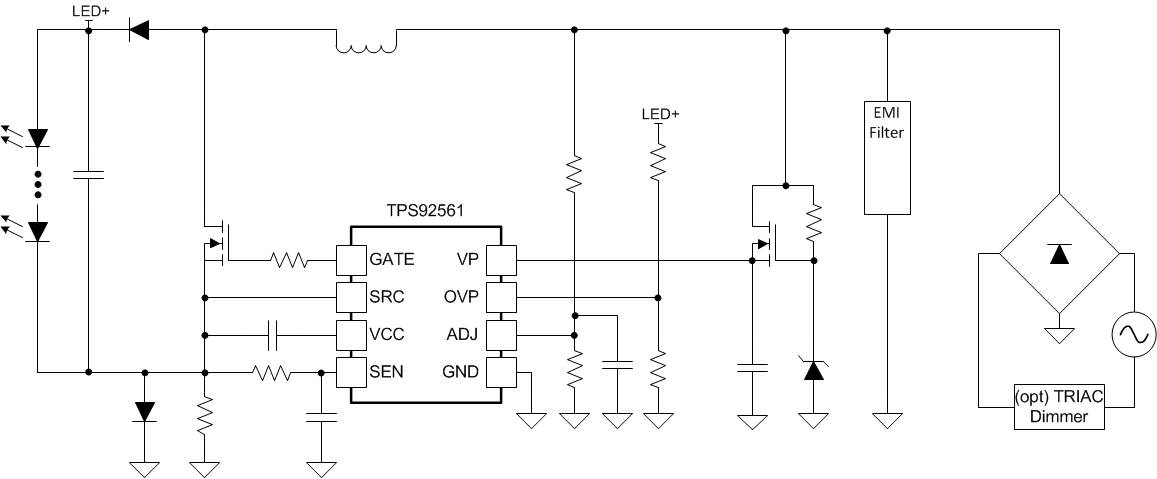
Typical Application Schematic

4 Revision History
Changes from B Revision (January 2014) to C Revision
- Added ESD Ratings table, Feature Description section, Device Functional Modes, Application and Implementation section, Power Supply Recommendations section, Layout section, Device and Documentation Support section, and Mechanical, Packaging, and Orderable Information section. Go
Changes from A Revision (December 2013) to B Revision
- Removed product preview bannerGo
Changes from * Revision (December 2013) to A Revision
- Updated figure to add AR111 lamps for closed-loop regulated e-transformer compatible, non-TRIAC dimmable boost for AR111 and MR16 lampsGo