-
TPS92690 N-Channel Controller for Dimmable LED Drives With Low-Side Current Sense
- 1 Features
- 2 Applications
- 3 Description
- 4 Revision History
- 5 Pin Configuration and Functions
- 6 Specifications
-
7 Detailed Description
- 7.1 Overview
- 7.2 Functional Block Diagram
- 7.3
Feature Description
- 7.3.1 Current Regulators
- 7.3.2 Peak Current Mode Control
- 7.3.3 Switching Frequency and Synchronization
- 7.3.4 Current Sense and Current Limit
- 7.3.5 Average LED Current
- 7.3.6 Precision Reference (VREF)
- 7.3.7 Low-Level Analog Dimming
- 7.3.8 Soft-Start and Shutdown
- 7.3.9 VCC Regulator and Start-Up
- 7.3.10 Overvoltage Protection (OVP)
- 7.3.11 Input Undervoltage Lockout (UVLO)
- 7.3.12 PWM Dimming
- 7.3.13 Control Loop Compensation
- 7.3.14 Thermal Shutdown
- 7.4 Device Functional Modes
-
8 Application and Implementation
- 8.1 Application Information
- 8.2
Typical Applications
- 8.2.1
Basic Topology Schematics
- 8.2.1.1 Design Requirements
- 8.2.1.2
Detailed Design Procedure
- 8.2.1.2.1 Operating Point
- 8.2.1.2.2 Switching Frequency
- 8.2.1.2.3 Average LED Current
- 8.2.1.2.4 Inductor Ripple Current
- 8.2.1.2.5 Output Capacitance
- 8.2.1.2.6 Peak Current Limit
- 8.2.1.2.7 Loop Compensation
- 8.2.1.2.8 Input Capacitance
- 8.2.1.2.9 NFET
- 8.2.1.2.10 Diode
- 8.2.1.2.11 Input UVLO
- 8.2.1.2.12 Output OVLO
- 8.2.1.3 Application Curve
- 8.2.2
Simplified Application
- 8.2.2.1 Design Requirements
- 8.2.2.2
Detailed Design Procedure
- 8.2.2.2.1 Operating Point
- 8.2.2.2.2 Switching Frequency
- 8.2.2.2.3 Average LED Current
- 8.2.2.2.4 Inductor Ripple Current
- 8.2.2.2.5 LED Ripple Current
- 8.2.2.2.6 Peak Current Limit
- 8.2.2.2.7 Loop Compensation
- 8.2.2.2.8 Input Capacitance
- 8.2.2.2.9 NFET
- 8.2.2.2.10 Diode
- 8.2.2.2.11 Output OVLO
- 8.2.2.2.12 Input UVLO
- 8.2.2.2.13 Soft-Start
- 8.2.2.2.14 PWM Dimming Method
- 8.2.2.2.15 Analog Dimming Method
- 8.2.1
Basic Topology Schematics
- 9 Power Supply Recommendations
- 10Layout
- 11Device and Documentation Support
- 12Mechanical, Packaging, and Orderable Information
- IMPORTANT NOTICE
Package Options
Mechanical Data (Package|Pins)
- PWP|16
Thermal pad, mechanical data (Package|Pins)
- PWP|16
Orderable Information
TPS92690 N-Channel Controller for Dimmable LED Drives With Low-Side Current Sense
1 Features
- Input Voltage Range from 4.5 to 75 V
- Adjustable Current Sense (50 to 500 mV)
- Low-Side Current Sensing
- 2-Ω MOSFET Gate Driver
- Input Undervoltage Protection
- Output Overvoltage Protection
- Cycle-by-Cycle Current Limit
- PWM Dimming Input
- Programmable Oscillator Frequency
- External Synchronization Capability
- Slope Compensation
- Programmable Soft-Start Function
- HTSSOP (PWP), 16-Pin, Exposed Pad Package
2 Applications
- LED Drivers
- Constant Current Regulator: Boost, Cuk, Flyback, and SEPIC
3 Description
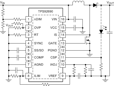
The TPS92690 device is a high-voltage, low-side NFET controller with an adjustable output current sense resistor voltage. Ideal for LED drivers, it contains all of the features needed to implement current regulators based on boost, SEPIC, flyback, and Cuk topologies.
Output current regulation is based on peak current-mode control supervised by a control loop. This methodology eases the design of loop compensation while providing inherent input voltage feed-forward compensation. The TPS92690 device includes a high-voltage start-up regulator that operates over a wide input range between 4.5 and 75 V. The PWM controller is designed for high-speed capability including an oscillator frequency range up to 2 MHz. The TPS92690 device includes an error amplifier, precision reference, cycle-by-cycle current limit, and thermal shutdown.
Device Information(1)
| PART NUMBER | PACKAGE | BODY SIZE (NOM) |
|---|---|---|
| TPS92690 | HTSSOP (16) | 5.00 mm × 4.40 mm |
- For all available packages, see the orderable addendum at the end of the data sheet.
Simplified Application

4 Revision History
Changes from * Revision (December 2012) to A Revision
- Added ESD Ratings table, Feature Description section, Device Functional Modes section, Application and Implementation section, Power Supply Recommendations section, Layout section, Device and Documentation Support section, and Mechanical, Packaging, and Orderable Information sectionGo
- Separated data sheet from TPS92690-Q1. For the TPS92690-Q1 data sheet, see SLVSCU0 on www.ti.com.Go
5 Pin Configuration and Functions

Pin Functions
| PIN | TYPE | DESCRIPTION | |
|---|---|---|---|
| NAME | NO. | ||
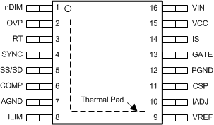
| AGND | 7 | GND | Connect to PGND through DAP exposed thermal pad for proper ground return path. |
| COMP | 6 | I | Connect ceramic capacitor to GND to set loop compensation. |
| CSP | 11 | I | Connect to positive terminal of sense resistor in series with LED stack. |
| GATE | 13 | O | Connect to main N-channel MOSFET gate of switching converter. |
| IADJ | 10 | I | Connect resistor divider from VREF to set error amplifier reference voltage. |
| ILIM | 8 | I | Connect resistor divider from VREF to set current limit threshold voltage at IS pin. |
| IS | 14 | I | Connect to drain of main N-channel MOSFET or to source of MOSFET if sense resistor is used for improved accuracy. |
| nDIM | 1 | I | Connect resistor divider from VIN to set UVLO threshold and hysteresis. Connect through diode or MOSFET to PWM dim concurrently. |
| OVP | 2 | I | Connect resistor divider from output voltage to set OVP threshold and hysteresis. |
| PGND | 12 | GND | Connect to AGND through the exposed thermal pad for proper ground return path. |
| RT | 3 | O | Connect resistor to AGND to set base switching frequency. |
| SS/SD | 5 | I | Connect capacitor to AGND to set soft-start delay. Pull pin below 75 mV for low-power shutdown. |
| SYNC | 4 | I | Connect external PWM signal to set switching frequency. Must be higher than base frequency set at RT pin. Can also connect series resistor and capacitor to drain of main MOSFET and capacitor to AGND to implement zero-crossing detection for quasi-resonant topologies. In either case, a falling edge on SYNC triggers a new on-time at GATE. If tied to ground, internal oscillator is used. |
| VCC | 15 | O | Bypass with 2.2-µF ceramic capacitor to provide bias supply for controller. |
| VIN | 16 | I | Connect to input supply of converter. Bypass with 100-nF ceramic capacitor to AGND as close to the device as possible. |
| VREF | 9 | O | Connect to the IADJ pin directly or through resistor divider. Bypass with 100-nF ceramic capacitor to AGND. |
| Thermal Pad | GND | ||