SLUSC82A March 2015 – March 2015 UCC24630
PRODUCTION DATA.
- 1 Features
- 2 Applications
- 3 Description
- 4 Revision History
- 5 Pin Configuration and Functions
- 6 Specifications
- 7 Detailed Description
- 8 Application and Implementation
- 9 Power Supply Recommendations
- 10Layout
- 11Device and Documentation Support
- 12Mechanical, Packaging, and Orderable Information
- 13Mechanical, Packaging, and Orderable Information
Package Options
Mechanical Data (Package|Pins)
- DBV|6
Thermal pad, mechanical data (Package|Pins)
Orderable Information
1 Features
- Secondary-Side SR Controller Optimized for 5-V to 24-V Flyback Systems
- Operating Frequency Up to 200 kHz
- Volt-Second Balance SR On-Time Control
- Minimize Effect of MOSFET Device and Layout Inductance
- CCM Operation Compatibility
- Compatible with PSR and SSR Control
- Auto Low-Power Detect and 110-µA Standby Mode Current
- Wide VDD Range from 3.6 V to 28 V
- Rail-to-Rail Gate Driver with 13-V Clamp
- Open and Short Pin Fault Protection
2 Applications
3 Description
The UCC24630 SR controller is a high-performance controller and driver for N-channel MOSFET power devices used for secondary-side synchronous rectification.
The combination of controller and MOSFET emulates a near-ideal diode rectifier. This solution not only directly reduces power dissipation of the rectifier but also reduces primary-side losses as well, due to compounding of efficiency gains.
Utilizing a volt-second balancing control method, the UCC24630 is ideal for flyback power supplies over a wide-output voltage range since the device is not connected directly to the MOSFET drain. The SR drive turn-off threshold is not dependent on the MOSFET RDS(on) which allows optimizing for maximum conduction time. Also secondary current ringing due to device and layout inductance does not affect the SR turn-off threshold.
The UCC24630 controller offers a programmable false-trigger filter, a frequency detector to automatically switch to standby mode during low power conditions and pin fault protections. The UCC24630 is compatible with DCM, TM and CCM operation.
The wide VDD operating range, wide programming range of the VPC voltage and blanking time, allows use in a variety of flyback converter designs.
Device Information(1)
| PART NUMBER | PACKAGE | BODY SIZE (NOM) |
|---|---|---|
| UCC24630 | SOT23 (6) | 2.92 mm x 1.30 mm |
- For all available packages, see the orderable addendum at the end of the data sheet.
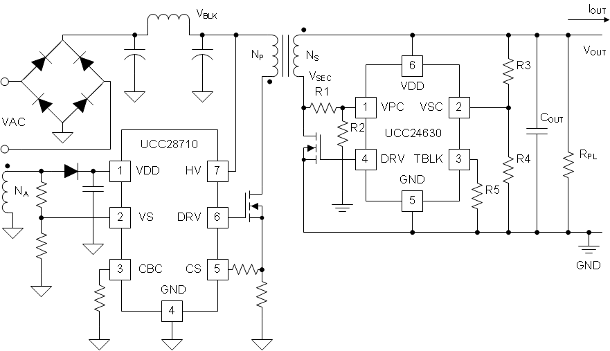
Simplified Schematic

Gate-Drive Timing vs VDS Sensing SR Driver
