-
UCC24636 Synchronous Rectifier (SR) Controller With Ultra-Low Standby Current
- 1 Features
- 2 Applications
- 3 Description
- 4 Revision History
- 5 Device Comparison Table
- 6 Pin Configuration and Functions
- 7 Specifications
- 8 Detailed Description
- 9 Application and Implementation
- 10Power Supply Recommendations
- 11Layout
- 12Device and Documentation Support
- 13Mechanical, Packaging, and Orderable Information
- IMPORTANT NOTICE
Package Options
Mechanical Data (Package|Pins)
- DBV|6
Thermal pad, mechanical data (Package|Pins)
Orderable Information
UCC24636 Synchronous Rectifier (SR) Controller With Ultra-Low Standby Current
1 Features
- Secondary-Side SR Controller Optimized for 5-V to 24-V Output Discontinuous/Transition Mode Only Flyback Converters
- Volt-Second Balance Control Enables Highest Rectifier Efficiency
- Compatible with PSR and SSR Flyback Controllers
- Ultra Low 110-µA Standby Current Consumption
- Auto-Detect Standby Mode Disables SR Switching for Lower No-Load Power Consumption
- SR Turn-Off Independent of RDSON and Parasitic Inductance
- Operating Frequency Up to 130 kHz
- Wide VDD Range from 3.6 V to 28 V
- Adaptive Gate Drive Clamp
- Open and Short Pin Fault Protection
2 Applications
- AC/DC Adapters For Smartphones and Tablets
- USB Chargers with Type-C Connectors
- Notebook and Ultrabook Adapters
- High Efficiency Flyback Converters in Industrial SMPS
- High Efficiency Auxilliary Power In Server and Desktop Applications
3 Description
The UCC24636 SR is a compact, 6-pin secondary-side synchronous rectifier MOSFET controller and driver for high efficiency Flyback converters operating in Discontinuous (DCM) and Transition mode (TM). Unlike traditional SR controllers which measure the SR MOSFET drain voltage, UCC24636 implements a volt-second balance control method to determine the turn off transition of the SR MOSFET; hence, SR conduction time is independent of the MOSFET RDSON, parasitic inductance or ringing allowing flexibility to designers in component slelction and PCB layout. This control method enables maximum SR conduction time and highest rectifier efficiency for a given MOSFET.
The controller has built in intelligence to detect converter no load operation and automatically enters standby mode. While in standby mode, it disables the SR MOSFET and lowers its bias supply current to 110uA to further reduce overall system standby power consumption. The wide VDD operating range for the controller allows direct bias from the converter output for fixed or variable output voltage designs. This eliminates the need for an auxilliary winding on the main transformer, which simplifies the circuit design and reduces the cost.
Device Information(1)
| PART NUMBER | PACKAGE | BODY SIZE (NOM) |
|---|---|---|
| UCC24636 | SOT23 (6) | 2.92 mm x 1.30 mm |
- For all available packages, see the orderable addendum at the end of the data sheet.
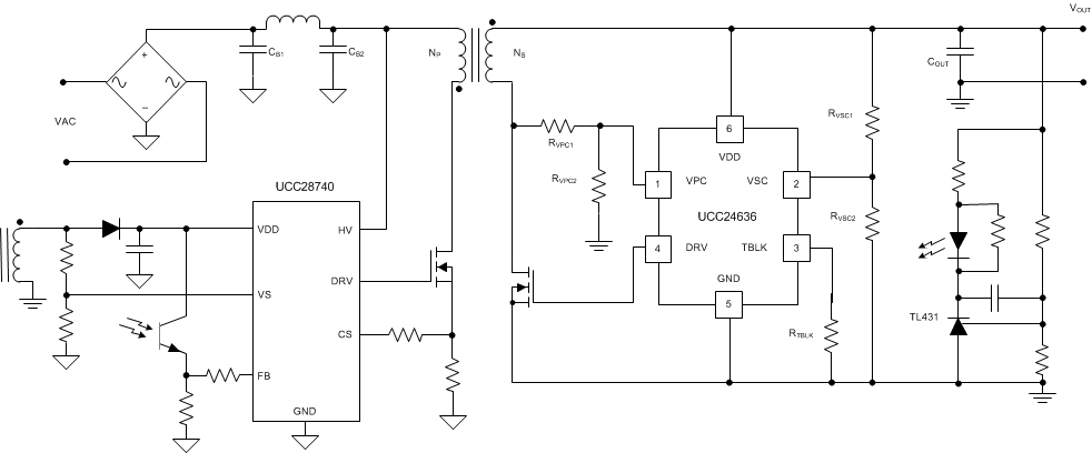
Simplified Schematic

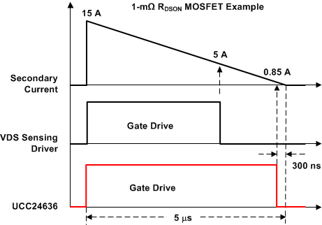
Gate-Drive Timing vs VDS Sensing SR Driver

4 Revision History
Changes from * Revision (December 2015) to A Revision
- Changed device status from Product Preview to Production Data and released full data sheet.Go
5 Device Comparison Table
| PART NUMBER | CCM DEAD TIME CONTROL | tOFF (µs) | FSW(MAX) (kHz) |
|---|---|---|---|
| UCC24636 | No | 4.35 | 130 |
| UCC24630 | Yes | 2.5 | 200 |
6 Pin Configuration and Functions

Pin Functions
| PIN | I/O(1) | DESCRIPTION | |
|---|---|---|---|
| NO. | NAME | ||
| 1 | VPC | I | The Voltage during Primary Conduction pin is connected to a resistor divider from the SR MOSFET drain. This pin determines a sample of the primary-side MOSFET volt seconds during the primary on-time. This voltage programs a voltage controlled current source for the internal VPC ramp charging current. |
| 2 | VSC | I | The Voltage during Secondary Conduction pin is connected to a resistor divider from the power-supply output. This pin determines a sample of the secondary-side output voltage used to determine SR MOSFET conduction time. This voltage programs a voltage controlled current source for the internal VSC ramp charging current. |
| 3 | TBLK | – | TIME BLANK pin is used to select the blanking time of the VPC rising edge. A programmable range from 200 ns to 2 µs is available to prevent false detection of the primary on-time due to ringing during DCM operation. |
| 4 | DRV | O | DRIVE is an output used to drive the gate of an external synchronous rectifier N-channel MOSFET switching transistor, with source pin connected to GND. |
| 5 | GND | G | The GROUND pin is both the reference pin for the controller and the low-side return for the drive output. Special care should be taken to return all AC decoupling capacitors as close as possible to this pin and avoid any common trace length with analog signal return paths. |
| 6 | VDD | P | VDD is the bias supply input pin to the controller. A carefully placed bypass capacitor to GND is required on this pin. |