Menu
Product
Email
PDF
Order now
UCC27288 3-A 120-V Half-Bridge Driver with 8-V UVLO and External Bootstrap Diode
SLUSE21B
June 2020 – April 2022
UCC27288
PRODUCTION DATA
CONTENTS
SEARCH
UCC27288 3-A 120-V Half-Bridge Driver with 8-V UVLO and External Bootstrap Diode
1
Features
2
Applications
3
Description
4
Revision History
5
Pin Configuration and Functions
6
Specifications
6.1
Absolute Maximum Ratings
6.2
ESD Ratings
6.3
Recommended Operating Conditions
6.4
Thermal Information
6.5
Electrical Characteristics
6.6
Switching Characteristics
6.7
Typical Characteristics
7
Detailed Description
7.1
Overview
7.2
Functional Block Diagram
7.3
Feature Description
7.3.1
Start-up and UVLO
7.3.2
Input Stages
7.3.3
Level Shifter
7.3.4
Output Stage
7.3.5
Negative Voltage Transients
7.4
Device Functional Modes
8
Application and Implementation
8.1
Application Information
8.2
Typical Application
8.2.1
Design Requirements
8.2.2
Detailed Design Procedure
8.2.2.1
Select Bootstrap and VDD Capacitor
8.2.2.2
External Bootstrap Diode and Series Resistor
8.2.2.3
Estimate Driver Power Losses
8.2.2.4
Selecting External Gate Resistor
8.2.2.5
Delays and Pulse Width
8.2.2.6
VDD and Input Filter
8.2.2.7
Transient Protection
8.2.3
Application Curves
9
Power Supply Recommendations
10
Layout
10.1
Layout Guidelines
10.2
Layout Example
11
Device and Documentation Support
11.1
Receiving Notification of Documentation Updates
11.2
Support Resources
11.3
Trademarks
11.4
Electrostatic Discharge Caution
11.5
Glossary
12
Mechanical, Packaging, and Orderable Information
IMPORTANT NOTICE
Package Options
Mechanical Data (Package|Pins)
D|8
MSOI002K
Thermal pad, mechanical data (Package|Pins)
Orderable Information
sluse21b_oa
search
No matches found.
Full reading width
Full reading width
Comfortable reading width
Expanded reading width
Card for each section
Card with all content
DATA SHEET
UCC27288 3-A 120-V Half-Bridge Driver with 8-V UVLO and External Bootstrap Diode
1
Features
Drives two N-channel MOSFETs in high-side low-side configuration
16-ns typical propagation delay
12-ns rise, 10-ns typical fall time with 1800-pF load
1-ns typical delay matching
Configurable external bootstrap diode
8-V typical undervoltage lockout
Absolute maximum negative voltage handling on inputs (–5 V)
Absolute maximum negative voltage handling on HS (–14 V)
±3-A peak output current
Absolute maximum boot voltage 120 V
Inputs are independent of each other and VDD
Under voltage lockout for both channels
Specified from –40°C to
140°C
junction temperature
2
Applications
Solar power optimizer
Merchant network & server PSU
Merchant telecom rectifiers
DC input BLDC motor drive
Test & measurement equipment
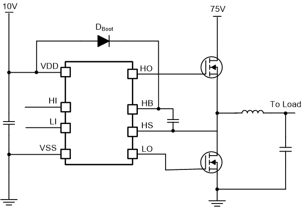
Simplified Application Diagram