UCC2751x Single-Channel, High-Speed, Low-Side Gate Driver (With 4-A Peak Source and 4-A Peak Sink)
1 Features
- Low-Cost Gate-Driver Device Offering Superior Replacement of NPN and PNP Discrete Solutions
- 4-A Peak-Source and 4-A Peak-Sink Symmetrical Drive
- Fast Propagation Delays (13-ns Typical)
- Fast Rise and Fall Times (9-ns and 7-ns Typical)
- 4.5 to 18-V Single-Supply Range
- Outputs Held Low During VDD UVLO (Ensures Glitch-Free Operation at Power Up and Power Down)
- TTL and CMOS Compatible Input-Logic Threshold (Independent of Supply Voltage)
- Hysteretic-Logic Thresholds for High-Noise Immunity
- Dual Input Design (Choice of an Inverting (IN– pin) or Noninverting (IN+ Pin) Driver Configuration)
- Unused Input Pin Can Be Used for Enable or Disable Function
- Output Held Low When Input Pins Are Floating
- Input Pin Absolute Maximum Voltage Levels Not Restricted by VDD Pin Bias Supply Voltage
- Operating Temperature Range of –40°C to 140°C
- 5-Pin DBV (SOT-23) and 6-Pin DRS (3-mm ×
3-mm WSON With Exposed Thermal Pad) Package Options
2 Applications
- Switched-Mode Power Supplies
- DC-DC Converters
- Companion Gate-Driver Devices for Digital-Power Controllers
- Solar Power, Motor Control, UPS
- Gate Driver for Emerging Wide Band-Gap Power Devices (such as GaN)
3 Description
The UCC27516 and UCC27517 single-channel, high-speed, low-side gate driver devices can effectively drive MOSFET and IGBT power switches. Using a design that inherently minimizes shoot-through current, UCC27516 and UCC27517 can source and sink high peak-current pulses into capacitive loads offering rail-to-rail drive capability and extremely small propagation delay, typically 13 ns.
The UCC27516 and UCC27517 provides 4-A source, 4-A sink (symmetrical drive) peak-drive current capability at VDD = 12 V.
Device Information(1)
| PART NUMBER | PACKAGE | BODY SIZE (NOM) |
|---|---|---|
| UCC27516 | SON (6) | 3.00 mm × 3.00 mm |
| UCC27517 | SOT-23 (5) | 2.90 mm × 1.60 mm |
- For all available packages, see the orderable addendum at the end of the datasheet.
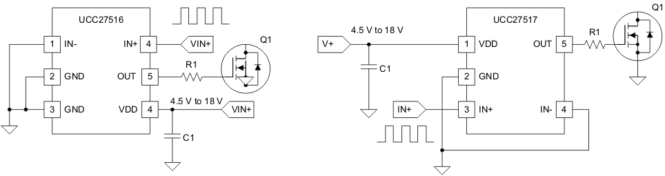
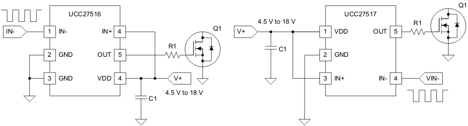
Typical Application Diagrams
4 Revision History
Changes from C Revision (May 2013) to D Revision
- Added Pin Configuration and Functions section, ESD Ratings table, Feature Description section, Device Functional Modes, Application and Implementation section, Power Supply Recommendations section, Layout section, Device and Documentation Support section, and Mechanical, Packaging, and Orderable Information section Go
Changes from B Revision (June 2012) to C Revision
- Added 0.5 to beginning of PSW equation in Power Dissipation section Go
Changes from A Revision (March 2012) to B Revision
- Added UCC27516 device.Go
- Added GND, ground definition.Go
- Added DC and repetitive pulse rates to OUT voltage.Go
- Added note 5.Go
- Changed Human Body Model max value from 2000 V to 400V.Go
- Changed Charged Device Model max value from 500 V to 100 V.Go
- Added UCC27516 block diagram.Go
- Added PCB layout bullet.Go
- Added Thermal Information description.Go
5 Description (continued)
The UCC27516 and UCC27517 are designed to operate over a wide VDD range of 4.5 to 18 V and wide temperature range of –40°C to 140°C. Internal undervoltage lockout (UVLO) circuitry on the VDD pin holds output low outside VDD operating range. The capability to operate at low voltage levels such as below 5 V, along with best-in-class switching characteristics, is especially suited for driving emerging wide band-gap power-switching devices such as GaN power semiconductor devices.
The UCC27516 and UCC27517 devices feature a dual-input design which offers flexibility of implementing both inverting (IN– pin) and noninverting (IN+ pin) configurations with the same device. Either the IN+ or IN- pin can be used to control the state of the driver output. The unused input pin can be used for enable and disable function. For safety purpose, internal pullup and pulldown resistors on the input pins ensure that outputs are held low when input pins are in floating condition. Hence the unused input pin is not left floating and must be properly biased to ensure that driver output is in enabled for normal operation.
The input pin threshold of the UCC27516 and UCC27517 devices are based on TTL and CMOS compatible low-voltage logic which is fixed and independent of the VDD supply voltage. Wide hysteresis between the high and low thresholds offers excellent noise immunity.
6 Device Comparison Table
The UCC2751x family of gate-driver products (Table 1) represent TI’s latest generation of single-channel low-side high-speed gate-driver devices featuring high-source/sink current capability, industry best-in-class switching characteristics and a host of other features (Table 2), all of which combine to ensure efficient, robust, and reliable operation in high-frequency switching power circuits.
Table 1. UCC2751x Product Family Summary
| PART NUMBER | PACKAGE | PEAK CURRENT (SOURCE/SINK) | INPUT THRESHOLD LOGIC |
|---|---|---|---|
| UCC27516DRS | 3 mm × 3 mm WSON, 6 pin | 4-A/8-A (Symmetrical Drive) |
CMOS/TTL-Compatible (low voltage, independent of VDD bias voltage) |
| UCC27511DBV | SOT-23, 6 pin | ||
| UCC27516DRS | 3 mm × 3 mm WSON, 6 pin | 4-A/4-A (Symmetrical Drive) |
|
| UCC27517DBV | SOT-23, 5 pin | ||
| UCC27518DBV | SOT-23, 5 pin | CMOS (follows VDD bias voltage) |
|
| UCC27519DBV | SOT-23, 5 pin |
7 Pin Configuration and Functions
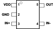
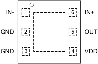
Pin Functions – UCC27516
| PIN | I/O | DESCRIPTION | |
|---|---|---|---|
| NO. | NAME | ||
| 1 | IN– | I | Inverting Input: When the driver is used in noninverting configuration, connect IN- to GND in order to enable output, OUT held LOW if IN- is unbiased or floating. |
| 2, 3 | GND | — | Ground: All signals referenced to this pin. TI recommends to connect pin 2 and pin 3 on PCB as close to the device as possible. |
| 4 | VDD | I | Bias supply input. |
| 5 | OUT | I | Sourcing/Sinking Current Output of Driver |
| 6 | IN+ | O | Noninverting Input: When the driver is used in inverting configuration, connect IN+ to VDD in order to enable output, OUT held LOW if IN+ is unbiased or floating. |
Pin Functions – UCC27517
8 Specifications
8.1 Absolute Maximum Ratings(1)(2)(3)
over operating free-air temperature range (unless otherwise noted)| MIN | MAX | UNIT | |||
|---|---|---|---|---|---|
| Supply voltage | VDD | –0.3 | 20 | V | |
| OUT voltage | DC | –0.3 | VDD + 0.3 | ||
| Repetitive pulse less than 200 ns(5) | –2 | VDD + 0.3 | |||
| Output continuous current | IOUT_DC (source/sink) | 0.3 | A | ||
| Output pulsed current (0.5 µs) | IOUT_pulsed(source/sink) | 4 | |||
| IN+, IN-(4) | –0.3 | 20 | V | ||
| Operating virtual junction temperature, TJ | –40 | 150 | °C | ||
| Lead temperature | Soldering, 10 sec. | 300 | |||
| Reflow | 260 | ||||
| Storage temperature, Tstg | –65 | 150 | |||
8.2 ESD Ratings
| VALUE | UNIT | |||
|---|---|---|---|---|
| V(ESD) | Electrostatic discharge | Human body model (HBM), per ANSI/ESDA/JEDEC JS-001(1) | ±4000 | V |
| Charged-device model (CDM), per JEDEC specification JESD22-C101(2) | ±1000 | |||
8.3 Recommended Operating Conditions
over operating free-air temperature range (unless otherwise noted)| MIN | NOM | MAX | UNIT | |
|---|---|---|---|---|
| Supply voltage range, VDD | 4.5 | 12 | 18 | V |
| Operating junction temperature range | –40 | 140 | °C | |
| Input voltage, IN+ and IN- | 0 | 18 | V |
8.4 Thermal Information
| THERMAL METRIC(1) | UCC27516 | UCC27517 | UNIT | |
|---|---|---|---|---|
| WSON | SOT-23 | |||
| 6 PINS | 5 PINS | |||
| RθJA | Junction-to-ambient thermal resistance | 85.6 | 217.6 | °C/W |
| RθJC(top) | Junction-to-case (top) thermal resistance | 100.1 | 85.8 | |
| RθJB | Junction-to-board thermal resistance | 58.6 | 44.0 | |
| ψJT | Junction-to-top characterization parameter | 7.5 | 4.0 | |
| ψJB | Junction-to-board characterization parameter | 58.7 | 43.2 | |
| RθJC(bot) | Junction-to-case (bottom) thermal resistance | 23.7 | n/a | |
8.5 Electrical Characteristics
VDD = 12 V, TA = TJ = –40°C to 140°C, 1-µF capacitor from VDD to GND. Currents are positive into, negative out of the specified pin.| PARAMETER | TEST CONDITIONS | MIN | TYP | MAX | UNIT | ||
|---|---|---|---|---|---|---|---|
| BIAS CURRENTS | |||||||
| IDD(off) | Startup current | VDD = 3.4 V | IN+ = VDD, IN- = GND | 40 | 100 | 160 | µA |
| IN+ = IN- = GND or IN+ = IN- = VDD | 25 | 75 | 145 | ||||
| IN+ = GND, IN- = VDD | 20 | 60 | 115 | ||||
| UNDERVOLTAGE LOCKOUT (UVLO) | |||||||
| VON | Supply start threshold | TA = 25°C | 3.91 | 4.20 | 4.5 | V | |
| TA = –40°C to 140°C | 3.70 | 4.20 | 4.65 | ||||
| VOFF | Minimum operating voltage after supply start | 3.45 | 3.9 | 4.35 | |||
| VDD_H | Supply voltage hysteresis | 0.2 | 0.3 | 0.5 | |||
| INPUTS (IN+, IN-) | |||||||
| VIN_H | Input signal high threshold | Output high for IN+ pin, Output low for IN- pin |
2.2 | 2.4 | V | ||
| VIN_L | Input signal low threshold | Output low for IN+ pin, Output high for IN- pin |
1.0 | 1.2 | |||
| VIN_HYS | Input signal hysteresis | 1.0 | |||||
| SOURCE/SINK CURRENT | |||||||
| ISRC/SNK | Source/sink peak current(1) | CLOAD = 0.22 µF, FSW = 1 kHz | ±4 | A | |||
| OUTPUTS (OUT) | |||||||
| VDD-VOH | High output voltage | VDD = 12 V IOUT = –10 mA |
50 | 90 | mV | ||
| VDD = 4.5 V IOUT = –10 mA |
60 | 130 | |||||
| VOL | Low output voltage | VDD = 12 IOUT = 10 mA |
5 | 10 | |||
| VDD = 4.5 V IOUT = 10 mA |
6 | 12 | |||||
| ROH | Output pullup resistance(2) | VDD = 12 V IOUT = –10 mA |
5.0 | 7.5 | Ω | ||
| VDD = 4.5 V IOUT = –10 mA |
5.0 | 11.0 | |||||
| ROL | Output pulldown resistance | VDD = 12 V IOUT = 10 mA |
0.5 | 1.0 | |||
| VDD = 4.5 V IOUT = 10 mA |
0.6 | 1.2 | |||||
8.6 Switching Characteristics
over operating free-air temperature range (unless otherwise noted)| PARAMETER | TEST CONDITIONS | MIN | TYP | MAX | UNIT | |
|---|---|---|---|---|---|---|
| tR | Rise time(1) | VDD = 12 V CLOAD = 1.8 nF |
8 | 12 | ns | |
| VDD = 4.5 V CLOAD = 1.8 nF |
16 | 22 | ||||
| tF | Fall time(1) | VDD = 12 V CLOAD = 1.8 nF |
7 | 11 | ||
| VDD=4.5V CLOAD = 1.8 nF |
7 | 11 | ||||
| tD1 | IN+ to output propagation delay(1) | VDD = 12 V 5-V input pulse CLOAD = 1.8 nF |
4 | 13 | 23 | |
| VDD = 4.5 V 5-V input pulse CLOAD = 1.8 nF |
4 | 15 | 26 | |||
| tD2 | IN- to output propagation delay(1) | VDD = 12 V CLOAD = 1.8 nF |
4 | 13 | 23 | |
| VDD = 4.5 V CLOAD = 1.8 nF |
4 | 19 | 30 | |||

8.7 Typical Characteristics
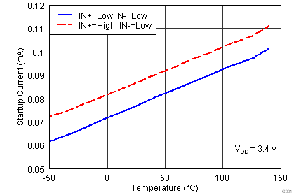 Figure 5. Startup Current vs Temperature
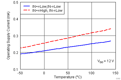 Figure 7. Supply Current vs Temperature (Output In DC On/Off Condition)
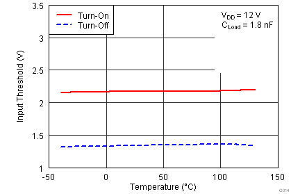 Figure 9. Input Threshold vs Temperature
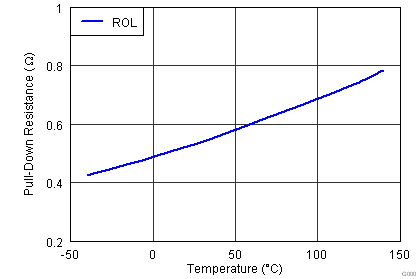 Figure 11. Output Pulldown Resistance vs Temperature
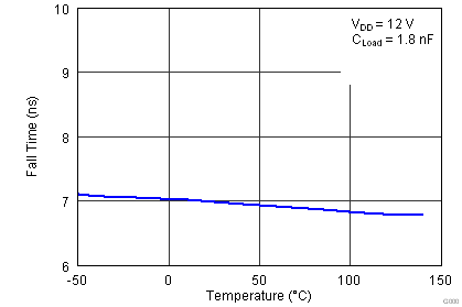 Figure 13. Fall Time vs Temperature
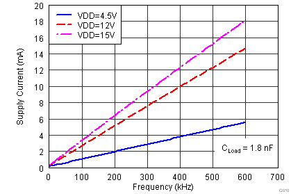 Figure 15. Operating Supply Current vs Frequency
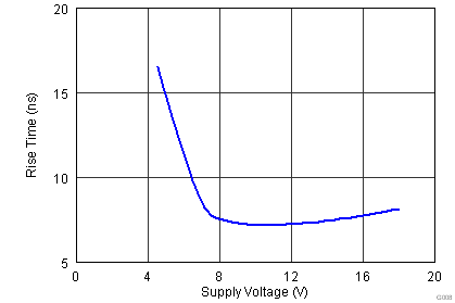 Figure 17. Rise Time vs Supply Voltage
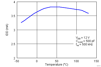 Figure 6. Operating Supply Current vs Temperature (Output Switching)
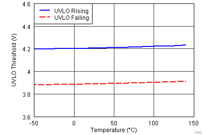 Figure 8. UVLO Threshold Voltage vs Temperature
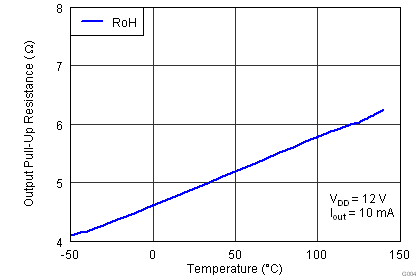 Figure 10. Output Pullup Resistance vs Temperature
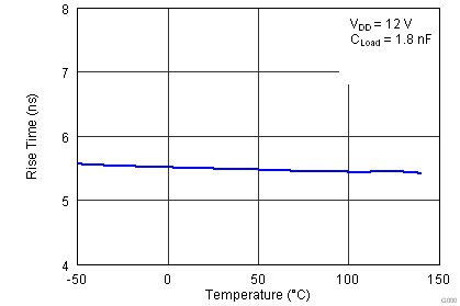 Figure 12. Rise Time vs Temperature
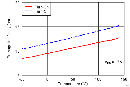 Figure 14. Input To Output Propagation Delay vs Temperature
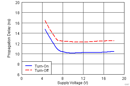 Figure 16. Propagation Delays vs Supply Voltage
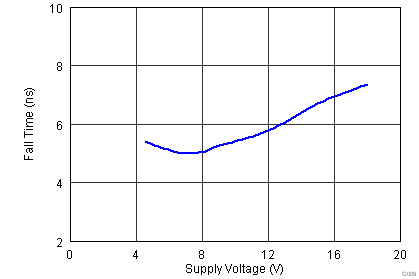 Figure 18. Fall Time vs Supply Voltage
9 Detailed Description
9.1 Overview
The UCC2751x single-channel, high-speed, low-side gate-driver device can effectively drive MOSFET and IGBT power switches. Using a design that inherently minimizes shoot-through current, the UCC2751x device can source and sink high peak-current pulses into capacitive loads, offering rail-to-rail drive capability and extremely small propagation delay of 13 ns (typical). The UCC2751x device provides 4-A source, 4-A sink (symmetrical drive) peak-drive current capability. The UCC27511 device is designed to operate over a wide VDD range of 4.5 to 18 V, and a wide temperature range of –40°C to 140°C.
Internal UVLO circuitry on the VDD pin holds the output low outside VDD operating range. The capability to operate at low voltage levels, such as below 5 V, along with best-in-class switching characteristics, is suited for driving emerging wide band-gap power-switching devices such as GaN power-semiconductor devices.
The UCC2751x device features a dual-input design which offers flexibility of implementing both inverting (IN– pin) and noninverting (IN+ pin) configuration with the same device. Either the IN+ or IN– pin can be used to control the state of the driver output. The unused input pin can be used for enable and disable functions. For system robustness, internal pullup and pulldown resistors on the input pins ensure that outputs are held low when the input pins are in floating condition. Therefore the unused input pin is not left floating and must be properly biased to ensure that driver output is in enabled for normal operation. The input pin threshold of the device is based on TTL and CMOS-compatible low-voltage logic which is fixed and independent of the VDD supply voltage. Wide hysteresis between the high and low thresholds offers excellent noise immunity.
Table 2. UCC2751x Family of Features and Benefits
| FEATURE | BENEFIT |
|---|---|
| High Source/Sink Current Capability 4 A/8 A (Asymmetrical) – UCC27511/2 4 A/4 A (Symmetrical) – UCC2751x |
High current capability offers flexibility in employing UCC2751x family of devices to drive a variety of power switching devices at varying speeds |
| Best-in-class 13-ns (typ) Propagation delay | Extremely low-pulse transmission distortion |
| Expanded VDD Operating range of 4.5 V to 18 V | Flexibility in system design Low VDD operation ensures compatibility with emerging wide-bandgap power devices such as GaN |
| Expanded Operating Temperature range of -40°C to 140°C (See Electrical Characteristics table) |
|
| VDD UVLO Protection | Outputs are held low in UVLO condition, which ensures predictable glitch-free operation at power up and power down |
| Outputs held low when input pins (INx) in floating condition | Safety feature, especially useful in passing abnormal condition tests during safety certification |
| Ability of input pins (and enable pin in UCC27518/9) to handle voltage levels not restricted by VDD pin bias voltage | System simplification, especially related to auxiliary bias supply architecture |
| Split output structure in UCC27511 (OUTH, OUTL) | Allows independent optimization of turnon and turnoff speeds |
| Strong sink current (8 A) and low pulldown impedance (0.375 Ω) in UCC27511/2 | High immunity to C x dV/dt Miller turnon events |
| CMOS/TTL compatible input threshold logic with wide hysteresis in UCC27511/2/6/7 | Enhanced noise immunity, while retaining compatibility with microcontroller logic-level input signals (3.3 V, 5 V) optimized for digital power |
| CMOS input threshold logic in UCC27518/9 (VIN_H – 70% VDD, VIN_L – 30% VDD) | Well suited for slow input-voltage signals, with flexibility to program delay circuits (RCD) |
9.2 Functional Block Diagrams
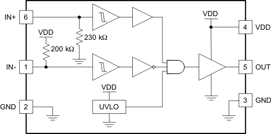 Figure 19. UCC27516 Functional Block Diagram

9.3 Feature Description
9.3.1 VDD and Undervoltage Lockout
The UCC2751x devices have internal UVLO protection feature on the VDD-pin supply-circuit blocks. Whenever the driver is in UVLO condition (for example when VDD voltage is less than VON during power up and when VDD voltage is less than VOFF during power down), this circuit holds all outputs LOW, regardless of the status of the inputs. The UVLO is typically 4.2 V with 300-mV typical hysteresis. This hysteresis helps prevent chatter when low VDD-supply voltages have noise from the power supply and also when there are droops in the VDD-bias voltage when the system commences switching and there is a sudden increase in IDD. The capability to operate at low voltage levels such as below 5 V, along with best-in-class switching characteristics, is especially suited for driving emerging GaN wide-bandgap power-semiconductor devices.
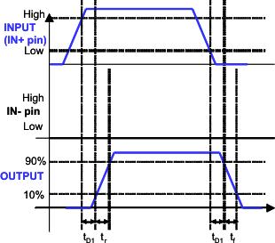
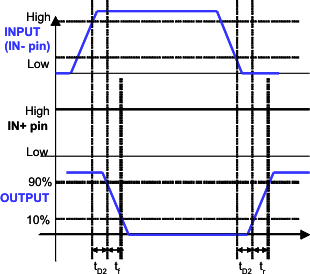
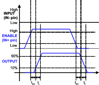
For example, at power up, the UCC2751x driver output remains LOW until the VDD voltage reaches the UVLO threshold. The magnitude of the OUT signal rises with VDD until steady-state VDD is reached. In the noninverting operation (PWM signal applied to IN+ pin) shown below, the output remains LOW until the UVLO threshold is reached, and then the output is in-phase with the input. In the inverting operation (PWM signal applied to IN- pin) shown below the output remains LOW until the UVLO threshold is reached, and then the output is out-phase with the input. In both cases, the unused input pin must be properly biased to enable the output. Note that in these devices the output turns to high-state only if IN+ pin is high and IN- pin is low after the UVLO threshold is reached.
Because the driver draws current from the VDD pin to bias all internal circuits, for the best high-speed circuit performance, two VDD bypass capacitors are recommended to prevent noise problems. The use of surface-mount components is highly recommended. A 0.1-μF ceramic capacitor should be located as close as possible to the VDD to GND pins of the gate driver. In addition, a larger capacitor (such as 1 μF) with relatively low ESR should be connected in parallel and close proximity, in order to help deliver the high-current peaks required by the load. The parallel combination of capacitors should present a low impedance characteristic for the expected current levels and switching frequencies in the application.
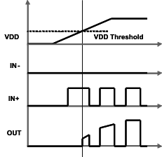 Figure 21. Power Up (Noninverting Drive)
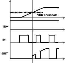 Figure 22. Power Up (Inverting Drive)
9.3.2 Operating Supply Current
The UCC2751x features very low quiescent IDD currents. The typical operating-supply current in Undervoltage-Lockout (UVLO) state and fully-on state (under static and switching conditions) are summarized in Figure 5, Figure 6, and Figure 7. The IDD current when the device is fully on and outputs are in a static state (DC high or DC low, see Figure 7) represents lowest quiescent IDD current when all the internal logic circuits of the device are fully operational. The total supply current is the sum of the quiescent IDD current, the average IOUT current due to switching and finally any current related to pullup resistors on the unused input pin. For example when the inverting input pin is pulled low additional current is drawn from VDD supply through the pullup resistors (refer to Functional Block Diagrams for the device Block Diagram). Knowing the operating frequency (fSW) and the MOSFET gate (QG) charge at the drive voltage being used, the average IOUT current can be calculated as product of QG and fSW.
A complete characterization of the IDD current as a function of switching frequency at different VDD bias voltages under 1.8-nF switching load is provided in Figure 15. The strikingly-linear variation and close correlation with theoretical value of average IOUT indicates negligible shoot-through inside the gate-driver device attesting to the high-speed characteristics of IOUT.
9.3.3 Input Stage
The input pins of the UCC27516 and UCC27517 devices are based on a TTL/CMOS compatible input-threshold logic that is independent of the VDD supply voltage. With typ high threshold = 2.2 V and typ low threshold = 1.2 V, the logic-level thresholds can be conveniently driven with PWM-control signals derived from 3.3-V and 5-V digital-power controllers. Wider hysteresis (typ 1 V) offers enhanced noise immunity compared to traditional TTL-logic implementations, where the hysteresis is typically less than 0.5 V. These devices also feature tight control of the input-pin threshold-voltage levels which eases system-design considerations and ensures stable operation across temperature. The very low input capacitance on these pins reduces loading and increases switching speed.
The device features an important safety function wherein, whenever any of the input pins are in a floating condition, the output of the respective channel is held in the low state. This is achieved using VDD-pullup resistors on all the inverting inputs (IN- pin) or GND-pulldown resistors on all the noninverting input pins (IN+ pin), (refer to Functional Block Diagrams).
The device also features a dual-input configuration with two input pins available to control the state of the output. The user has the flexibility to drive the device using either a noninverting input pin (IN+) or an inverting input pin (IN-). The state of the output pin is dependent on the bias on both the IN+ and IN- pins. Refer to the input/output logic truth table (Table 3) and the Typical Application Diagrams, (Figure 24 and Figure 25), for additional clarification.
Once an input pin has been chosen for PWM drive, the other input pin (the unused input pin) must be properly biased in order to enable the output. As mentioned earlier, the unused input pin cannot remain in a floating condition because, whenever any input pin is left in a floating condition, the output is disabled for safety purposes. Alternatively, the unused input pin can effectively be used to implement an enable and disable function, as explained below.
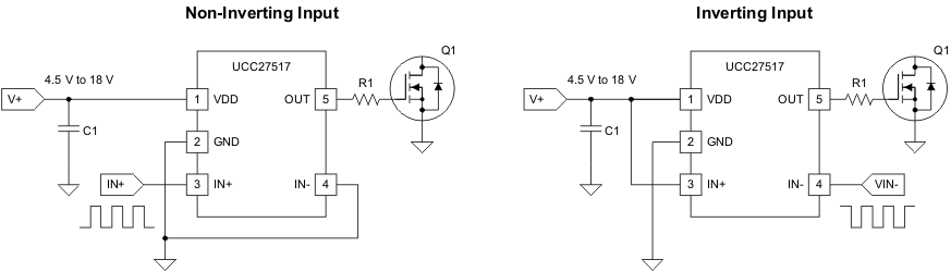
- To drive the device in a noninverting configuration, apply the PWM-control input signal to IN+ pin. In this case, the unused input pin, IN-, must be biased low (eg. tied to GND) in order to enable the output.
- Alternately, the IN- pin can be used to implement the enable/disable function using an external logic signal. OUT is disabled when IN- is biased high and OUT is enabled when IN- is biased low.
- To drive the device in an inverting configuration, apply the PWM-control input signal to IN- pin. In this case, the unused input pin, IN+, must be biased high (eg. tied to VDD) in order to enable the output.
- Alternately, the IN+ pin can be used to implement the enable/disable function using an external logic signal. OUT is disabled when IN+ is biased low and OUT is enabled when IN+ is biased high.
- Finally, note that the output pin is driven into a high state only when IN+ pin is biased high and IN- input is biased low.
The input stage of the driver should preferably be driven by a signal with a short rise or fall time. Caution must be exercised whenever the driver is used with slowly-varying input signals, especially in situations where the device is located in a mechanical socket or PCB layout is not optimal:
- High dI/dt current from the driver output coupled with board layout parasitics causes ground bounce. Because the device features just one GND pin, which may be referenced to the power ground, the differential voltage between input pins and GND is modified and triggers an unintended change of output state. Because of fast 13-ns propagation delay, high-frequency oscillations ultimately occur, which increases power dissipation and poses risk of damage.
- 1-V input-threshold hysteresis boosts noise immunity compared to most other industry-standard drivers.
- In the worst case, when a slow input signal is used and PCB layout is not optimal, adding a small capacitor (1 nF) between input pin and ground very close to the driver device is necessary. This helps to convert the differential mode noise with respect to the input-logic circuitry into common-mode noise and avoid unintended change of output state.
If limiting the rise or fall times to the power device is the primary goal, then an external resistance is highly recommended between the output of the driver and the power device instead of adding delays on the input signal. This external resistor has the additional benefit of reducing part of the gate charge related power dissipation in the gate-driver device package and transferring the gate driver into the external resistor.
9.3.4 Enable Function
As mentioned earlier, an enable/disable function is easily implemented in the UCC27516 and UCC27517 using the unused input pin. When IN+ is pulled down to GND or IN- is pulled down to VDD, the output is disabled. Thus IN+ pin is used like an enable pin that is based on active-high logic, while IN- can be used like an enable pin that is based on active-low logic.
9.3.5 Output Stage
The UCC27516 and UCC27517 devices can deliver 4-A source, 4-A sink (symmetrical drive) at VDD = 12 V. The output stage of the UCC27516 and UCC27517 devices are illustrated in Figure 23. The UCC27516 and UCC27517 devices features a unique architecture on the output stage which delivers the highest peak-source current when most needed during the Miller-plateau region of the power-switch turnon transition (when the power-switch drain/collector voltage experiences dV/dt). The device output stage features a hybrid pullup structure using a parallel arrangement of N-Channel and P-Channel MOSFET devices. By turning on the N-Channel MOSFET during a narrow instant when the output changes state from low to high, the gate-driver device delivers a brief boost in the peak-sourcing current enabling fast turnon.
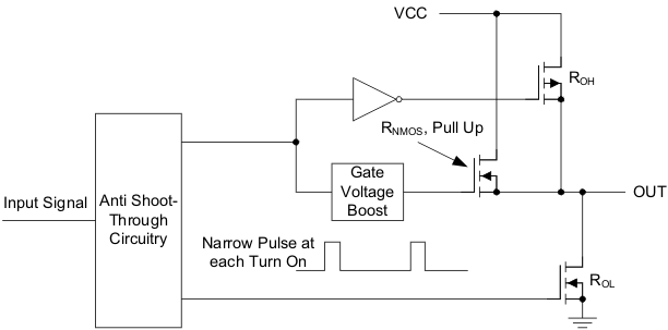 Figure 23. UCC2751x Gate Driver Output Structure
The ROH parameter (see Electrical Characteristics) is a DC measurement and is representative of the on-resistance of the P-Channel device only, because the N-Channel device is turned on only during output change of state from low to high. Thus the effective resistance of the hybrid pullup stage is much lower than what is represented by ROH parameter. The pulldown structure is composed of a N-Channel MOSFET only. The ROL parameter (see Electrical Characteristics), which is also a DC measurement, is representative of true impedance of the pulldown stage in the device. In the UCC27516 and UCC27517, the effective resistance of the hybrid pullup structure is approximately 1.4 × ROL.
The driver-output voltage swings between VDD and GND providing rail-to-rail operation because of the MOS output stage which delivers very low dropout. The presence of the MOSFET-body diodes also offers low impedance to switching overshoots and undershoots. This means that in many cases, external Schottky-diode clamps may be eliminated. The outputs of these drivers are designed to withstand 500-mA reverse current without either damage to the device or logic malfunction.
9.3.6 Low Propagation Delays
The UCC27516 and UCC27517 driver devices feature best-in-class input-to-output propagation delay of 13 ns (typ) at VDD = 12 V. This promises the lowest level of pulse-transmission distortion available from industry-standard gate-driver devices for high-frequency switching applications. As seen in Figure 14, there is very little variation of the propagation delay with temperature and supply voltage as well, offering typically less than 20-ns propagation delays across the entire range of application conditions.
10 Application and Implementation
NOTE
Information in the following applications sections is not part of the TI component specification, and TI does not warrant its accuracy or completeness. TI’s customers are responsible for determining suitability of components for their purposes. Customers should validate and test their design implementation to confirm system functionality.
10.1 Application Information
High-current gate-driver devices are required in switching power applications for a variety of reasons. In order to effect fast switching of power devices and reduce associated switching power losses, a powerful gate driver is employed between the PWM output of controllers and the gates of the power-semiconductor devices. Further, gate drivers are indispensable when there are times that the PWM controller cannot directly drive the gates of the switching devices. With advent of digital power, this situation is often encountered because the PWM signal from the digital controller is often a 3.3-V logic signal, which is not capable of effectively turning on a power switch. A level-shifting circuitry is needed to boost the 3.3-V signal to the gate-drive voltage (such as 12 V) in order to fully turn on the power device and minimize conduction losses. Because traditional buffer-drive circuits based on NPN/PNP bipolar transistors in totem-pole arrangement, being emitter-follower configurations, lack level-shifting capability, the circuits prove inadequate with digital power. Gate drivers effectively combine both the level-shifting and buffer-drive functions. Gate drivers also find other needs such as minimizing the effect of high-frequency switching noise by locating the high-current driver physically close to the power switch, driving gate-drive transformers and controlling floating power-device gates, reducing power dissipation and thermal stress in controllers by moving gate-charge power losses into itself. Finally, emerging wide-bandgap power-device technologies, such as GaN based switches, which are capable of supporting very high switching frequency operation, are driving very special requirements in terms of gate-drive capability. These requirements include operation at low VDD voltages (5 V or lower), low propagation delays and availability in compact, low-inductance packages with good thermal capability. In summary gate-driver devices are extremely important components in switching power combining benefits of high-performance, low cost, component count and board space reduction with a simplified system design.
10.2 Typical Application
The UCC27516 and UCC27517 devices can be used in non-inverting and inverting driver configurations.
NOTE
The UCC27516 features two ground pins, pin 2 and pin 3. TI recommends tying both pins together using PCB trace as close as possible to the device.
10.2.1 Design Requirements
When selecting the proper gate driver device for an end application, some design considerations must be evaluated first to make the most appropriate selection. Among these considerations are input-to-output configuration, the input threshold type, bias supply voltage levels, peak source and sink currents, availability of independent enable and disable functions, propagation delay, power dissipation, and package type.
Table 4. Design Parameters
| Design Parameter | Example Value |
|---|---|
| Input-to-Output Logic | Non-Inverting |
| Input Threshold Type | Logic Level |
| VDD Bias Supply Voltage | 10 V (Minimum), 13 V (Nominal), 15 V (Peak) |
| Peak Source and Sink Currents | Minimum 3 A Source, Minimum 3 A Sink |
| Enable and Disable Function | Yes, Needed |
| Propagation Delay | Maximum 40 ns or less |
10.2.2 Detailed Design Procedure
10.2.2.1 Input-to-Output Logic
The design should specify which type of input-to-output configuration should be used. If turning on the power MOSFET or IGBT when the input signal is in high state is preferred, then the noninverting configuration must be selected. If turning off the power MOSFET or IGBT when the input signal is in high state is preferred, the inverting configuration must be chosen. The UCC27516 and UCC27517 devices can be configured in either an inverting or noninverting input-to-output configuration, using the IN– or IN+ pins, respectively. To configure the device for use in inverting mode, tie the IN+ pin to VDD and apply the input signal to the IN– pin. For the non inverting configuration, tie the IN– pin to GND and apply the input signal to the IN+ pin.
10.2.2.2 Input Threshold Type
The type of input voltage threshold determines the type of controller used with the gate driver device. The UCC27516 and UCC27517 devices feature a TTL and CMOS-compatible input threshold logic, with wide hysteresis. The threshold voltage levels are low voltage and independent of the VDD supply voltage, which allows compatibility with both logic-level input signals from microcontrollers, as well as higher-voltage input signals from analog controllers. See Electrical Characteristics for the actual input threshold voltage levels and hysteresis specifications for the UCC27516 and UCC27517 devices.
10.2.2.3 VDD Bias Supply Voltage
The bias supply voltage to be applied to the VDD pin of the device should never exceed the values listed in the Recommended Operating Conditions table. However, different power switches demand different voltage levels to be applied at the gate terminals for effective turnon and turnoff. With certain power switches, a positive gate voltage may be required for turnon and a negative gate voltage may be required for turnoff, in which case the VDD bias supply equals the voltage differential. With a wide operating range from 4.5 V to 18 V, the UCC27516 and UCC27517 devices can be used to drive a variety of power switches, such as Si MOSFETs (for example, VGS = 4.5 V, 10 V, 12 V), IGBTs (VGE = 15 V, 18 V), and wide-band gap power semiconductors (such as GaN, certain types of which allow no higher than 6 V to be applied to the gate terminals).
10.2.2.4 Peak Source and Sink Currents
Generally, the switching speed of the power switch during turnon and turnoff should be as fast as possible, to minimize switching power losses. The gate driver device must be able to provide the required peak current for achieving the targeted switching speeds for the targeted power MOSFET.
Using the example of a power MOSFET, the system requirement for the switching speed is typically described in terms of the slew rate of the drain-to-source voltage of the power MOSFET (such as dVDS/dt). For example, the system requirement might state that a SPP20N60C3 power MOSFET must be turned-on with a dVDS/dt of 20V/ns or higher, under a DC bus voltage of 400 V in a continuous-conduction-mode (CCM) boost PFC-converter application. This type of application is an inductive hard-switching application and reducing switching power losses is critical. This requirement means that the entire drain-to-source voltage swing during power MOSFET turnon event (from 400 V in the OFF state to VDS(on) in on state) must be completed in approximately 20 ns or less.
When the drain-to-source voltage swing occurs, the Miller charge of the power MOSFET (QGD parameter in SPP20N60C3 power MOSFET data sheet = 33 nC typical) is supplied by the peak current of gate driver. According to the power MOSFET inductive switching mechanism, the gate-to-source voltage of the power MOSFET at this time is the Miller plateau voltage, which is typically a few volts higher than the threshold voltage of the power MOSFET, VGS(TH). To achieve the targeted dVDS/dt, the gate driver must be capable of providing the QGD charge in 20 ns or less. In other words, a peak current of 1.65 A (= 33 nC / 20 ns) or higher must be provided by the gate driver. The UCC27516 and UCC27517 gate driver is capable of providing 4-A peak sourcing current, which exceeds the design requirement and has the capability to meet the switching speed needed.
The 2.4x overdrive capability provides an extra margin against part-to-part variations in the QGD parameter of the power MOSFET, along with additional flexibility to insert external gate resistors and fine tune the switching speed for efficiency versus EMI optimizations. However, in practical designs the parasitic trace inductance in the gate drive circuit of the PCB will have a definitive role to play on the power MOSFET switching speed. The effect of this trace inductance is to limit the dI/dt of the output current pulse of the gate driver.
To illustrate this, consider output current pulse waveform from the gate driver to be approximated to a triangular profile, where the area under the triangle (½ ×IPEAK × time) would equal the total gate charge of the power MOSFET (QG parameter in SPP20N60C3 power MOSFET datasheet = 87 nC typical).
If the parasitic trace inductance limits the dI/dt, then a situation may occur in which the full peak current capability of the gate driver is not fully achieved in the time required to deliver the QG required for the power MOSFET switching. In other words, the time parameter in the equation would dominate and the IPEAK value of the current pulse would be much less than the true peak current capability of the device, while the required QG is still delivered. Because of this, the desired switching speed may not be realized, even when theoretical calculations indicate the gate driver is capable of achieving the targeted switching speed. Thus, placing the gate driver device very close to the power MOSFET and designing a tight gate drive-loop with minimal PCB trace inductance is important to realize the full peak-current capability of the gate driver.
10.2.2.5 Enable and Disable Function
Certain applications demand independent control of the output state of the driver, without involving the input signal. A pin offering an enable and disable function achieves this requirement. The UCC27516 and UCC27517 devices offer two input pins, IN+ and IN–, both of which control the state of the output as listed in Table 3. Based on whether an inverting or non inverting input signal is provided to the driver, the appropriate input pin can be selected as the primary input for controlling the gate driver. The other unused input pin can be used for the enable and disable functionality. If the design does not require an enable function, the unused input pin can be tied to either the VDD pin (in case IN+ is the unused pin), or GND (in case IN– is unused pin) to ensure it does not affect the output status.
10.2.2.6 Propagation Delay
The acceptable propagation delay from the gate driver is dependent on the switching frequency at which it is used, and the acceptable level of pulse distortion to the system. The UCC27516 and UCC27517 devices feature industry best-in-class 13-ns (typical) propagation delays, which ensure very little pulse distortion and allow operation at very high-frequencies. See Switching Characteristics for the propagation and switching characteristics of the UCC27516 and UCC27517 devices.
10.2.3 Application Curves
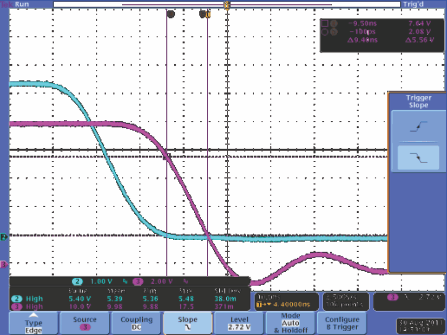
| VDD = 10 V | C(LOAD) = 1 nF |
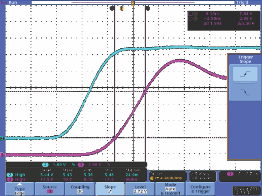
| VDD = 10 V | C(LOAD) = 1 nF |
11 Power Supply Recommendations
The bias supply voltage range for which the UCC27516 and UCC27517 device is rated to operate is from 4.5 V to 18 V. The lower end of this range is governed by the internal UVLO protection feature on the VDD pin supply circuit blocks. Whenever the driver is in UVLO condition when the VDD pin voltage is below the V(ON) supply start threshold, this feature holds the output low, regardless of the status of the inputs. The upper end of this range is driven by the 20-V absolute maximum voltage rating of the VDD pin of the device (which is a stress rating). Keeping a 2-V margin to allow for transient voltage spikes, the maximum recommended voltage for the VDD pin is 18 V.
The UVLO protection feature also involves a hysteresis function. This means that when the VDD pin bias voltage has exceeded the threshold voltage and the device begins to operate, and if the voltage drops, then the device continues to deliver normal functionality unless the voltage drop exceeds the hysteresis specification VDD(hys). While operating at or near the 4.5 V range, ensure that the voltage ripple on the auxiliary power supply output is smaller than the hysteresis specification of the device, to avoid triggering a device shutdown.
During system shutdown, the device operation continues until the VDD pin voltage has dropped below the V(OFF) threshold, which must be accounted for while evaluating system shutdown timing design requirements. Likewise, at system startup the device does not begin operation until the VDD pin voltage has exceeded above the V(ON) threshold. The quiescent current consumed by the internal circuit blocks of the device is supplied through the VDD pin. Keep in mind that the charge for source current pulses delivered by the OUT pin is also supplied through the same VDD pin. As a result, every time a current is sourced out of the output pin (OUT), a corresponding current pulse is delivered into the device through the VDD pin. Therefore, ensure that local bypass capacitors are provided between the VDD and GND pins, and located as close to the device as possible for the purpose of decoupling. A low ESR, ceramic surface mount capacitor is necessary. TI recommends using 2 capacitors; a 100-nF ceramic surface-mount capacitor which can be nudged very close to the pins of the device, and another surface-mount capacitor of few microfarads added in parallel.
12 Layout
12.1 Layout Guidelines
Proper PCB layout is extremely important in a high-current fast-switching circuit to provide appropriate device operation and design robustness. The UCC27516 and UCC27517 gate driver incorporates short-propagation delays and powerful output stages capable of delivering large current peaks with very fast rise and fall times at the gate of the power switch to facilitate voltage transitions very quickly. At higher VDD voltages, the peak-current capability is even higher (4-A/4-A peak current is at VDD = 12 V). Very high di/dt causes unacceptable ringing if the trace lengths and impedances are not well controlled. The following circuit layout guidelines are strongly recommended when designing with these high-speed drivers.
- Locate the driver device as close as possible to the power device in order to minimize the length of high-current traces between the output pins and the gate of the power device.
- Locate the VDD bypass capacitors between VDD and GND as close as possible to the driver with minimal trace length to improve the noise filtering. These capacitors support high-peak current being drawn from VDD during turnon of power MOSFET. The use of low inductance SMD components such as chip resistors and chip capacitors is highly recommended.
- The turnon and turnoff current-loop paths (driver device, power MOSFET and VDD bypass capacitor) should be minimized as much as possible in order to keep the stray inductance to a minimum. High dI/dt is established in these loops at two instances – during turnon and turnoff transients, which will induce significant voltage transients on the output pin of the driver device and gate of the power switch.
- Wherever possible parallel the source and return traces, taking advantage of flux cancellation.
- Separate power traces and signal traces, such as output and input signals.
- Star-point grounding is a good way to minimize noise coupling from one current loop to another. The GND of the driver should be connected to the other circuit nodes such as source of power switch or the ground of PWM controller at one, single point. The connected paths should be as short as possible to reduce inductance and be as wide as possible to reduce resistance.
- Use a ground plane to provide noise shielding. Fast rise and fall times at OUT may corrupt the input signals during transition. The ground plane must not be a conduction path for any current loop. Instead the ground plane must be connected to the star-point with one single trace to establish the ground potential. In addition to noise shielding, the ground plane can help in power dissipation as well.
- In noisy environments, tying the unused input pin of UCC27516 and UCC27517 to VDD (in case of IN+) or GND (in case of IN–) using short traces to ensure that the output is enabled and to prevent noise from causing malfunction in the output is necessary.
- The UCC27516 device offers two ground pins, pin 2 and pin 3. Shorting the two pins together using the PCB trace is extremely important. The shortest trace should be located as close as possible to the device.
12.2 Layout Example
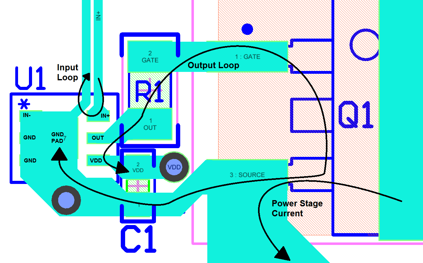 Figure 28. UCC27516DRS in Noninverting Configuration
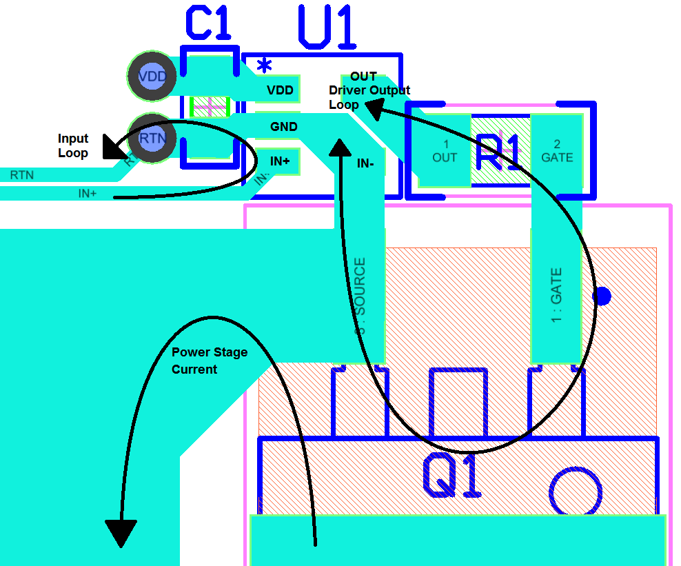 Figure 29. UCC27517DBV in Noninverting Configuration
12.3 Thermal Considerations
The useful range of a driver is greatly affected by the drive-power requirements of the load and the thermal characteristics of the package. For a gate driver to be useful over a particular temperature range the package must allow for the efficient removal of the heat produced while keeping the junction temperature within rated limits. The thermal metrics for the driver package is summarized in Thermal Information. For detailed information regarding the thermal information table, refer to the Application Note from Texas Instruments entitled IC Package Thermal Metrics (SPRA953).
The UCC27516 and UCC27517 devices are offered in SOT-23, 5-pin package (DBV) and 3 mm × 3 mm, WSON 6-pin package with exposed thermal pad (DRS), respectively. The Thermal Information table summarizes the thermal performance metrics related to the two packages. RθJA metric should be used for comparison of power dissipation between different packages. Under identical power dissipation conditions, the DRS package will maintain a lower die temperature than the DBV. The ψJT and ψJB metrics should be used when estimating the die temperature during actual application measurements.
The DRS is a better thermal package overall because of the exposed thermal pad and ability to sink heat to the PCB better than the DBV. The thermal pad in DRS package provides designers with an ability to create an excellent heat removal subsystem from the vicinity of the device, thus helping to maintain a lower junction temperature. This pad should be soldered to the copper on the printed circuit board directly underneath the device package. Then a printed circuit board designed with thermal lands and thermal vias completes a very efficient heat removal subsystem. In such a design, the heat is extracted from the semiconductor junction through the thermal pad, which is then efficiently conducted away from the location of the device on the PCB through the thermal network. This extraction helps to maintain a lower board temperature near the vicinity of the device leading to an overall lower device-junction temperature.
In comparison, for the DBV package, heat removal occurs primarily through the leads of the device and the PCB traces connected to the leads.
Note that the exposed pad in DRS package is not directly connected to any leads of the package. However, the DRS package is electrically and thermally connected to the substrate of the device which is the ground of the device. TI recommends to externally connect the exposed pads to GND in PCB layout for better EMI immunity.
12.4 Power Dissipation
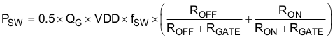
Power dissipation of the gate driver has two portions as shown in Equation 1.

The DC portion of the power dissipation is PDC = IQ x VDD where IQ is the quiescent current for the driver. The quiescent current is the current consumed by the device to bias all internal circuits such as input stage, reference voltage, logic circuits, protections, and also any current associated with switching of internal devices when the driver output changes state (such as charging and discharging of parasitic capacitances, parasitic shoot-through etc). The UCC27516 and UCC27517 features very low quiescent currents (less than 1 mA, refer Figure 7) and contains internal logic to eliminate any shoot-through in the output-driver stage. Thus the effect of the PDC on the total power dissipation within the gate driver can be safely assumed to be negligible.
The power dissipated in the gate-driver package during switching (PSW) depends on the following factors:
- Gate charge required of the power device (usually a function of the drive voltage VG, which is very close to input bias supply voltage VDD due to low VOH drop-out).
- Switching frequency.
- Use of external-gate resistors.
When a driver device is tested with a discrete, capacitive load calculating the power that is required from the bias supply is fairly easy. The energy that must be transferred from the bias supply to charge the capacitor is given by Equation 2.
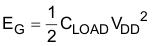
where
- CLOAD is load capacitor
- VDD is bias voltage feeding the driver
There is an equal amount of energy dissipated when the capacitor is charged. This leads to a total power loss given by Equation 3.
where
- ƒSW is the switching frequency
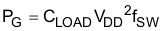
The switching load presented by a power MOSFET/IGBT is converted to an equivalent capacitance by examining the gate charge required to switch the device. This gate charge includes the effects of the input capacitance plus the added charge needed to swing the drain voltage of the power device as it switches between the ON and OFF states. Most manufacturers provide specifications of typical and maximum gate charge, in nC, to switch the device under specified conditions. Using the gate charge Qg, determine the power that must be dissipated when charging a capacitor. This is done by using the equation, QG = CLOAD x VDD, to provide Equation 4 for power:

This power PG is dissipated in the resistive elements of the circuit when the MOSFET/IGBT is being turned on or turned off. Half of the total power is dissipated when the load capacitor is charged during turnon, and the other half is dissipated when the load capacitor is discharged during turnoff. When no external gate resistor is employed between the driver and MOSFET/IGBT, this power is completely dissipated inside the driver package. With the use of external gate-drive resistors, the power dissipation is shared between the internal resistance of driver and external gate resistor in accordance to the ratio of the resistances (more power dissipated in the higher resistance component). Based on this simplified analysis, the driver power dissipation during switching is calculated in Equation 5.
13 Device and Documentation Support
13.1 Related Links
The table below lists quick access links. Categories include technical documents, support and community resources, tools and software, and quick access to sample or buy.
Table 5. Related Links
| PARTS | PRODUCT FOLDER | SAMPLE & BUY | TECHNICAL DOCUMENTS | TOOLS & SOFTWARE | SUPPORT & COMMUNITY |
|---|---|---|---|---|---|
| UCC27516 | Click here | Click here | Click here | Click here | Click here |
| UCC27517 | Click here | Click here | Click here | Click here | Click here |
13.2 Trademarks
All other trademarks are the property of their respective owners.
13.3 Electrostatic Discharge Caution

These devices have limited built-in ESD protection. The leads should be shorted together or the device placed in conductive foam during storage or handling to prevent electrostatic damage to the MOS gates.
13.4 Glossary
SLYZ022 — TI Glossary.
This glossary lists and explains terms, acronyms, and definitions.
14 Mechanical, Packaging, and Orderable Information
The following pages include mechanical, packaging, and orderable information. This information is the most current data available for the designated devices. This data is subject to change without notice and revision of this document. For browser-based versions of this data sheet, refer to the left-hand navigation.