UCC2751x Single-Channel, High-Speed, Low-Side Gate Driver (Based On CMOS Input Threshold With 4-A Peak Source and 4-A Peak Sink)
1 Features
- Low-Cost, Gate-Driver Device Offering Superior Replacement of NPN and PNP Discrete Solutions
- Pin-to-Pin Compatible With TI's TPS2828 and TPS2829 devices
- 4-A Peak Source and 4-A Peak Sink Symmetrical Drive
- Fast Propagation Delays (17-ns Typical)
- Fast Rise and Fall Times (8-ns and 7-ns Typical)
- 4.5-V to 18-V Single Supply Range
- Outputs Held Low During VDD UVLO (Ensures Glitch-Free Operation at Power Up and Power Down)
- CMOS Input Logic Threshold (Function of Supply Voltage With Hysteresis)
- Hysteretic Logic Thresholds for High Noise Immunity
- EN Pin for Enable Function (Allowed to Be No Connect)
- Output Held Low when Input Pins are Floating
- Input Pin Absolute Maximum Voltage Levels Not Restricted by VDD Pin Bias Supply Voltage
- Operating Temperature Range of –40°C to 140°C
- 5-Pin DBV Package (SOT-23)
2 Applications
- Switched-Mode Power Supplies
- DC-DC Converters
- Companion Gate Driver Devices for Digital Power Controllers
- Solar Power, Motor Control, UPS
- Gate Driver for Emerging Wide Band-Gap Power Devices (Such as GaN)
3 Description
The UCC27518 and UCC27519 single-channel, high-speed, low-side gate driver device can effectively drive MOSFET and IGBT power switches. Using a design that inherently minimizes shoot-through current, UCC27518 and UCC27519 can source and sink high, peak-current pulses into capacitive loads offering rail-to-rail drive capability and extremely small propagation delay typically 17 ns.
The UCC27518 and UCC27519 provide 4-A source, 4-A sink (symmetrical drive) peak-drive current capability at VDD = 12 V.
The UCC27518 and UCC27519 are designed to operate over a wide VDD range of 4.5 V to 18 V and a wide temperature range of –40°C to 140°C. Internal under voltage lockout (UVLO) circuitry on the VDD pin holds output low outside VDD operating range. The capability to operate at low voltage levels such as below 5 V, along with best-in-class switching characteristics, is especially suited for driving emerging wide band-gap power switching devices such as GaN power semiconductor devices.
Device Information(1)
| PART NUMBER | PACKAGE | BODY SIZE (NOM) |
|---|---|---|
| UCC27518 | SOT-23 (5) | 2.90 mm × 1.60 mm |
| UCC27519 |
- For all available packages, see the orderable addendum at the end of the datasheet.
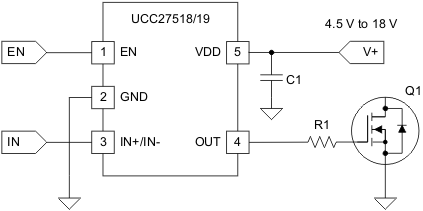
Typical Application Diagram
4 Revision History
Changes from * Revision (May 2012) to A Revision
- Added Pin Configuration and Functions section, ESD Ratings table, Feature Description section, Device Functional Modes, Application and Implementation section, Power Supply Recommendations section, Layout section, Device and Documentation Support section, and Mechanical, Packaging, and Orderable Information section Go
5 Description (continued)
The input pin threshold of the UCC27518 and UCC27519 are based on CMOS logic where the threshold voltage is a function of the VDD supply voltage. Typically Input High Threshold (VIN-H) is 55% VDD and Input Low Threshold (VIN-L) is 39% VDD. Wide hysteresis (16% VDD typically) between the high and low thresholds offers excellent noise immunity and lets users introduce delays using RC circuits between the input PWM signal and the INx pin of the device.
The UCC27518 and UCC27519 also feature a floatable enable function on the EN pin. The EN pin can be left in a no connect condition, which allows pin-to-pin compatibility between the UCC27518, UCC27519 and the TPS2828, TPS2829, respectively. The thresholds of the EN pin is a fixed voltage threshold and does not vary based on VDD pin bias voltage. Typically, the Enable High Threshold (VEN-H) is 2.1 V and Enable Low Threshold (VEN-L) is 1.25 V.