UCC2752x Dual 5-A High-Speed Low-Side Gate Driver Based on CMOS Input Threshold Logic
1 Features
- Industry-Standard Pin Out
- Two Independent Gate-Drive Channels
- 5-A Peak Source and Sink Drive Current
- CMOS Input Logic Threshold
(Function of Supply Voltage on VDD Pins) - Hysteretic Logic Thresholds for High Noise Immunity
- Independent Enable Function for Each Output
- Inputs and Enable Pin Voltage Levels Not Restricted by VDD Pin Bias Supply Voltage
- 4.5-V to 18-V Single Supply Range
- Outputs Held Low During VDD UVLO (Ensures Glitch-Free Operation at Power Up and Power Down)
- Fast Propagation Delays (17-ns Typical)
- Fast Rise and Fall Times (7-ns and 6-ns Typical)
- 1-ns Typical Delay Matching Between 2 Channels
- Outputs Held in Low When Inputs Floating
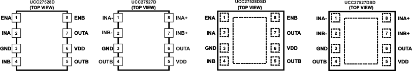
- SOIC-8, and 3-mm x 3-mm WSON-8 Package Options
- Operating Temperature Range of –40°C to 140°C
- –5-V Negative Voltage Handling Capability on Input Pins
2 Applications
- Switch-Mode Power Supplies
- DC-to-DC Converters
- Motor Control, Solar Power
- Gate Drive for Emerging Wideband Gap Power Devices Such as GaN
3 Description
The UCC2752x family of devices are dual-channel, high-speed, low-side gate driver devices capable of effectively driving MOSFET and IGBT power switches. Using a design that inherently minimizes shoot-through current, UCC2752x can deliver high-peak current pulses of up to 5-A source and 5-A sink into capacitive loads along with rail-to-rail drive capability and extremely small propagation delay typically 17 ns. In addition, the drivers feature matched internal propagation delays between the two channels which are very well suited for applications requiring dual-gate drives with critical timing, such as synchronous rectifiers. The input pin thresholds are based on CMOS logic, which is a function of the VDD supply voltage. Wide hysteresis between the high and low thresholds offers excellent noise immunity. The Enable pins are based on TTL and CMOS compatible logic, independent of VDD supply voltage.
Device Information(1)
| PART NUMBER | PACKAGE | BODY SIZE (NOM) |
|---|---|---|
| UCC27527 | WSON (8) | 3.00 mm x 3.00 mm |
| SOIC (8) | 4.90 mm x 3.91 mm | |
| UCC27528 | WSON (8) | 3.00 mm x 3.00 mm |
| SOIC (8) | 4.90 mm x 3.91 mm |
- For all available packages, see the orderable addendum at the end of the datasheet.
4 Revision History
Changes from D Revision (July 2013) to E Revision
- Added Handling Rating table, Feature Description section, Device Functional Modes, Application and Implementation section, Power Supply Recommendations section, Layout section, Device and Documentation Support section, and Mechanical, Packaging, and Orderable Information section Go
Changes from C Revision (June 2013) to D Revision
- Added OUTA, OUTB voltage field and values.Go
- Changed table note from "Values are verified by characterization and are not production tested." to "Values are verified by characterization on bench."Go
- Changed Bias Current TYP values from 170 µA to 180 µA.Go
Changes from B Revision (January 2013) to C Revision
- Changed UCC27527 packaging optionsGo
- Added UCC27527 Bias Current specifications.Go
- Added an updated Output Stage section.Go
- Added UCC2752X Gate Driver Output Structure imageGo
- Added updated Drive Current and Power Dissipation section.Go
- Added a PSW... equation.Go
Changes from A Revision (December 2012) to B Revision
- Changed Feature bullet from "-5-V Negative Voltage Handling Capability on Input and Enable Pins" to -5-V Negative Voltage Handling Capability on Input Pins"Go
Changes from * Revision (December 2012) to A Revision
5 Description (continued)
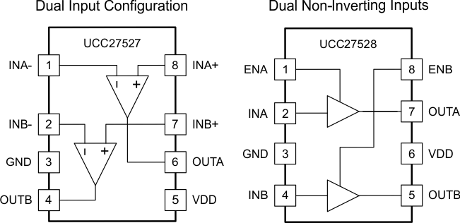
The UCC27528 is a dual noninverting driver. UCC27527 features a dual input design which offers flexibility of both inverting (IN– pin) and non-inverting (IN+ pin) configuration for each channel. Either IN+ or IN– pin can be used to control the state of the driver output. The unused input pin can be used for enable and disable functions. For safety purpose, internal pullup and pulldown resistors on the input pins of all the devices in UCC2752x family to ensure that outputs are held low when input pins are in floating condition. UCC27528 features Enable pins (ENA and ENB) to have better control of the operation of the driver applications. The pins are internally pulled up to VDD for active high logic and can be left open for standard operation.
6 Pin Configuration and Functions
Pin Functions (UCC27527)
| PIN | I/O | DESCRIPTION | |
|---|---|---|---|
| NUMBER | NAME | ||
| 1 | INA- | I | Inverting Input to Channel A: when Channel A is used in Non-Inverting configuration connect INA- to GND in order to Enable Channel A output, OUTA held low if INA- is unbiased or floating. |
| 2 | INB- | I | Inverting Input to Channel B: when Channel B is used in Non-Inverting configuration connect INB- to GND in order to Enable Channel B output, OUTB held low if INB- is unbiased or floating. |
| 3 | GND | – | Ground: All signals referenced to this pin. |
| 4 | OUTB | I | Output of Channel B |
| 5 | VDD | O | Bias Supply Input |
| 6 | OUTA | I | Output of Channel A |
| 7 | INB+ | O | Non-Inverting Input to Channel B: When Channel B is used in Inverting configuration connect INB+ to VDD in order to Enable Channel B output, OUTB held low if INB+ is unbiased or floating. |
| 8 | INA+ | I | Non-Inverting Input to Channel A: When Channel A is used in Inverting configuration connect INA+ to VDD in order to Enable Channel A output, OUTA held low if INA+ is unbiased or floating. |
Pin Functions (UCC27528)
| PIN | I/O | DESCRIPTION | |
|---|---|---|---|
| NUMBER | NAME | ||
| 1 | ENA | I | Enable input for Channel A: ENA biased low Disables Channel A output regardless of INA state, ENA biased high or floating Enables Channel A output, ENA allowed to float. |
| 2 | INA | I | Input to Channel A: Non-Inverting Input in UCC27528, OUTA held low if INA is unbiased or floating. |
| 3 | GND | – | Ground: All signals referenced to this pin. |
| 4 | INB | I | Input to Channel B: Non-Inverting Input in UCC27528, OUTB held low if INB is unbiased or floating. |
| 5 | OUTB | O | Output of Channel B |
| 6 | VDD | I | Bias supply input |
| 7 | OUTA | O | Output of Channel A |
| 8 | ENB | I | Enable input for Channel B: ENB biased low Disables Channel B output regardless of INB state, ENB biased high or floating Enables Channel B output, ENB allowed to float. |